

In Figure 9, the dotted purple line shows broadband noise suppression by filters, which is then increased again by the following amplifiers. The most important parameters that define broadband noise performance at the antenna are the maximum allowed gain for each amplifier stage, which also determines the power levels appearing at the filters.

Figure 9 Spectrum of the improved transmitter RF path.
It may be that the filter in front of the final power amplifier must handle a power level of some Watts due to the quite low allowed maximum gain of the amplifier following it. Such a high-power filter may be difficult to realize, especially because it must be tunable in frequency as well.
On the receiver side, a similar high-power filter may be required to ensure sufficient receiver performance in the presence of strong interferers. Therefore, the dual use of relevant resources like filters and other components for the receive and transmit paths should be considered during the process of optimizing the overall RF transceiver architecture.
The RF Generator (Exciter) is the Heart of the Radio
The most important building block of a transceiver is the RF generator (see Figure 10). It provides a low phase-noise modulated RF signal that represents the complete transmit signal of the transceiver. It starts with a sufficiently high level providing an already low broadband noise as a starting point to the following filter/amplifier chain of the transmit path. In receive, the unmodulated RF signal is either used as a local oscillator for superheterodyne receivers or is used as a clock signal for digital direct sampling receivers.

Figure 10 Transceiver RF generator.
Today it is technologically possible to realize the core part of the RF generator, represented by the box with the blue dotted lines in Figure 10, with a fully integrated solution. Even digital-analog converters (DACs) can be part of such a chip. Only some manufacturers are currently providing fully integrated solutions, but with a split between purely RF functionality and the core direct digital synthesizer (DDS), a sufficiently higher number of components is available.
The information signal (e.g. voice or data) to be transmitted is filtered and adjusted in level and is then digitized. The digitized signal passes through a baseband processing stage that creates a digital I/Q signal stream representing the modulation, including filtering. This digital I/Q modulation information is complex multiplied with the digital unmodulated carrier signal from the numerically controlled oscillator (NCO). This fully I/Q modulated digital RF signal is then input to a DAC and appears at its output as an analog RF signal to be transmitted.
Smart Power Control Loop
It is recommended to use a configuration for the RF generator where two parallel outputs are available, one with the modulated RF transmit signal and one with the unmodulated RF signal derived from the same digital oscillator. This second unmodulated signal is used to supply a feedback path for phase-coherent demodulation of the RF signal after the final power amplifier.
If this feedback signal is also provided, an I/Q data stream with the same format as the modulation stream, then an easy vectorial comparison of these two signals can be done. The comparison is first used to set up a power regulation loop by monitoring the level of the transmit signal. A second comparison checks the quality of the transmitted signal by comparing the I/Q constellation diagram of the transmit signal with the feedback signal. Active linearization can be used to pre-distort the transmit signal, compensating for all influences on the way to the antenna through all stages.
The block diagram of a high-end transmitter illustrating this optimized transmitter path is shown in Figure 11. The key element is still the RF generator as shown in Figure 10; however, the RF generator is now enhanced with an additional block providing the power regulation loop including an active linearization capability. The required feedback path and all associated signals are shown in purple, while the normal transmit path is shown in blue.

Figure 11 Optimized transmitter RF path.
The feedback demodulator is connected to the forward output of a directional coupler between the final amplifier and the antenna. If a second feedback demodulator is connected to the reflected output of the same directional coupler a highly capable analysis of all signal signals traveling from the antenna back to the final amplifier can be done. Due to the phase-coherent nature of the demodulation, it is now straightforward to distinguish between signals that are reflections of the transmit signal and those that have been received by the transmit antenna from other transmitters.
Signals from other transmitters are characterized by a frequency offset as compared to the transmit signal and can now be isolated. This enables an optimized strategy, keeping the transmit power constant or reducing it not more than necessary, independent of the source of the reflected signals.2
Always Design the Power Amplifier (PA) for Good Linearity
Active linearization is a regulation loop that compensates for the effects of nonlinearities of all elements between the RF generator and the antenna. It must be carefully designed with respect to its bandwidth otherwise it may increase the phase noise outside its bandwidth where broadband noise starts. Even when having such a capability available in a transmitter path, any amplifier should always be designed to provide good basic linearity.
Nonlinearities of amplifiers can be based on a variety of mechanisms and are often described with very complex formulas in the literature, but the practical view describing nonlinearities is much simpler. If, for example, a digitally modulated single carrier is used as a transmit signal, then linearity is just how fast and how accurate the output signal of an amplifier can follow the input signal in phase and amplitude.
Figure 12 shows a typical digitally modulated signal, like quadrature phase shift keying (QPSK). Within this simplified view it is easy to see what happens if an amplifier has no problem following phase changes of the modulation signal (shown in the blue circle) but does have a problem following amplitude changes (shown as red arrow). It may be that a basically linear Class AB amplifier appears to be nonlinear, but the real reason for this behavior is that the amplitude changes within the modulation signal are faster than the AM frequency response of the amplifier.

Figure 12 Phase and amplitude changes after an amplifier.
The AM frequency response of an amplifier is a major parameter in the context of nonlinearities and is set and limited in most cases by the circuitry of the input stages and not by the transistor. For a Class AB amplifier, the gate voltage may increase with an increasing RF drive signal and opens the transistor for a higher output power. This leads to a dynamic shift of bias toward Class A. It is important here that the average DC bias voltage at the gate follows the average level of the drive signal fast enough, otherwise, the output power of the transistor cannot follow amplitude changes at the input fast enough. Figure 13 shows a simplified circuit of a push-pull amplifier that may limit the AM frequency response.

Figure 13 Input circuit limiting AM frequency response.
The incoming signal is changed from unsymmetric to symmetric by the balanced-to- unbalanced (BALUN) device and relative to GND, one transistor is driven with the positive half of the RF carrier sinewave while the second transistor is driven with the negative half and vice versa. The envelope of the modulation signal represents the level of the RF carrier and should look identical on both gates. The average instantaneous level of the envelope is responsible for opening the gate to the required source gate voltage, shown as dotted lines in Figure 13.
The elements C1/C2 and R1/R2 set a low-pass characteristic. If the time constants are set too low, then the average DC voltage of fast modulation peaks cannot follow the fast changes of the envelope. Consequently, the gates are supplied with gate voltages that are too low (shown as red dotted lines) during fast modulation periods while the RF envelope reaches full amplitude.
This leads to the suppression of fast amplitude changes in the signals, which looks like amplifier saturation. This mechanism creates almost the same intermodulation distortion as a saturated amplifier, but it is simply caused by a bandwidth limitation of the DC paths within the input circuits of the PA.
The behavior of an amplifier with a limited AM frequency response may lead to an eye diagram showing strong inter-symbol interference (ISI) with memory effects in the time domain. Figure 14 shows an example of an eye diagram of a binary phase shift keyed (BPSK) signal when AM bandwidth limitation occurs.
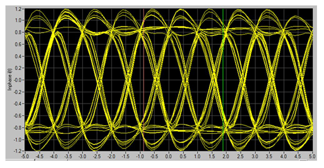
Figure 14 ICI caused by insufficient AM bandwidth.
ISI with memory effects may motivate some design engineers to compensate by using an active feedback loop implementing complex mathematical algorithms like the Volterra series and using a harmonic balance simulator for verification. It is therefore recommended to first optimize the AM frequency response of a PA according to the required bandwidth of the transmit signal and use the feedback loop for further optimization of the remaining nonlinear behavior if necessary.
The remaining signal distortion on the way to very high linearity may be complicated, like thermal effects which will then require complex mathematical solutions. In most cases, however, the linearity of an amplifier will be suitable for typical communication signals if the AM/FM frequency response is sufficiently high.
It is further recommended to design an amplifier for an AM/FM frequency bandwidth response that is at least two or three times higher than the highest modulation frequency of the signal to be transmitted. For an HF amplifier and SSB voice modulation, the AM frequency response should be at least 6 to 9 kHz. This method of improving the linearity of an amplifier is easily achieved and is easy to validate because only an AM signal is required for testing.
In a push-pull configuration, it is additionally important that the gates of both transistors see identical circuitry. In Figure 13, a DC path through the matching network connects the gates to both capacitors C3 and C4. It is likely that these capacitors have different values because they have been selected based on different goals; additionally, C4 is connected to a series impedance while C3 is directly connected to GND. As a result, the AM frequency responses at the two gates may be different from each other due to different capacitive loads. This leads to an unequal drive of the transistors. The circuitry can, therefore, not only ensure a sufficiently high AM frequency response but also an identical characteristic for each transistor.
With a good basic PA design, in combination with linearization, the following two-tone intermodulation values can be expected if the transmitter is driven with a two-tone signal leveled 6 dB below PEP for each tone. The IM3 values represent the difference between the intermodulation products and the two tones.
•IM3 ≥ 30 dB – basic linearity
•IM3 ≥ 40 dB – enhanced linearity using digital predistortion
•IM3 ≥ 45 dB – superior linearity using digital active linearization
Carefully designed in-band linearity of the transmitter chain enables good signal quality with respect to bit error rate (BER) or in-band signal-to-noise ratio (SNR). But even with very high linearity, beyond high-end requirements, some spectral regrowth may occur outside the transmission channel.
As a rule of thumb, the adjacent channel power (ACP) of a complex modulated single carrier waveform is typically lower than the in-channel power by the number of dBs expressed by the two-tone IM3. The out-of-channel spectral components will decrease in the same way as higher-order two-tone intermodulation products do.