

A Modern HF/VHF/UHF Transceiver for all Applications – What Would it Look Like Today?
Full Length Version of Article That Appeared in Oct Issue
Modern RF Transceivers represent more than just separated receiver and transmitter functionalities within the same box. In an operational scenario involving several transceivers, even a “perfect” receiver can demonstrate high-end performance only if the spectral purity of the transmit signals is sufficiently high. Therefore, a transceiver design must align major RF parameters and building blocks between transmit and receive paths to form a combined optimized transceiver architecture! In the following, a state-of-the-art “perfect” transceiver architecture is described. This is a full length version of the article that appeared in our Oct issue here.
When a receiver and transmitter are operated at different locations and far away from each other the only relevant receive parameter is sensitivity while the only relevant transmit parameter is output power. The closer a transmitter is to the receiver, the more significant are additional performance characteristics for both. While the receiver must increase its robustness to withstand the strong transmit signal at its front-end, the transmitter must increase its spectral purity to ensure that no spectral component from the transmit signal falls into an adjacent receive channel.
In some installations, transmit signals can be extremely strong at the receiver input, while their frequencies may also be simultaneously close to the receive channels. Overall system performance is determined by the minimum usable frequency offset between a transmit channel and a receive channel with a given decoupling between a receiver and a transmitter operating a given output power.
This so-called co-site situation directly influences the specifications, for example, the adjacent channel power ratio (ACPR) for the radio communication equipment. Within a particular frequency band and its typical applications, the operating parameters may lead to a totally different transceiver architecture when compared to different applications in other frequency bands. Consequently, a transceiver for a 5G mobile phone base station, for example, may look completely different than a mobile phone base station designed to operate in the HF, VHF or UHF Band.
While the best architecture for communication equipment in a particular frequency band may vary slightly, for simplicity we focus only on systems below 600 MHz.
DERIVATION OF KEY PARAMETERS FOR SPECIFICATIONS
The transceiver RF design is directly driven by some key parameters whose values and ranges strongly influence the required circuits and the concepts for major building blocks designed to meet system requirements. Therefore, it is highly recommended to define the worst-case system scenario with respect to RF power levels and frequency offsets and derive the key parameters from this setup.
It is reasonable to assume that such a system is built up using several transceivers of the same type that are operated either in a receive or transmit mode. This allows system performance to be enhanced by optimizing the receive and transmit paths as parts of a common transceiver RF architecture. Some building blocks will be shared between receive and transmit paths, which allows simplification of the overall architecture. Typical shareable building blocks may be analog RF filters and low-noise RF signal sources used for analog mixing or as clocks for signal processing stages.
Figure 1 is one example of a system setup. Based on the output power of the transmitter, total decoupling of the transmitter spectrum at the receiver input can be calculated (see Figure 2). This spectrum view is now the basis to derive further data for the receiver and the transmitter.

Figure 1 Co-location scenario for a transceiver.

Figure 2 Total spectrum at the receiver input.
If, for example, a desired sensitivity for the receiver without any interference from a transmitter is chosen, the corresponding noise figure (NF) for the receiver front-end can be calculated. The value of – 174 dBm/Hz represents the natural noise floor power spectral density (PSD) caused by thermal effects at room temperature (kT). The NF of the receiver is then converted into a noise floor density (NFD) as follows:
NFD = – 174 dBm/Hz + NF (in dB)(1)
This sets the reference for additional external noise generated by the transmitter, which reduces the sensitivity of the receiver by adding additional noise from outside. If the external NFD from the transmitter equals that of the receiver, then the sensitivity of the receiver is reduced by 3 dB. This is called the blocking effect, or reciprocal mixing if the transmitter is active. The use of NFD instead of NF (or levels for the desired receive signals) simplifies the so-called co-site calculation significantly. With this approach, it is not necessary to know all the details about the communication method used, not even knowledge about the bandwidth.
In an operational scenario, some performance parameters must be defined with respect to a minimum remaining sensitivity. A maximum level at the receiver front-end in the presence of a transmit signal at a minimum required frequency offset relative to the receive channel must be determined. The maximum level for the transmit signal at the receiver front-end is calculated from the transmitter output power in combination with the total decoupling (in dB) between the transmitter RF output connector and the receiver RF input connector.
SPECIFICATIONS FOR A HIGH-END TRANSCEIVER
Based on the above discussion, the most important RF requirements for a wideband transceiver are identified in Tables I and II to enable high-end system transceiver performance at a radio communication site. The RF architecture to be characterized is designed to meet these criteria.
This set of requirements demands very robust input stages to enable operation in a highly contested environment. These stages use filters and amplifiers in a cascaded configuration where some elements can be bypassed. As a result, the total receiver NF with all filters active is typically 4 to 6 dB higher than expected and is on the order of 10 dB. In situations where no strong interferers are present, some co-site filters can be bypassed and additional high gain amplifiers can be activated leading to NFs on the order of 4 dB or even less.1


WHAT ABOUT RECEIVER INTERMODULATION?
The specifications in Tables I and II do not show any values for receiver intermodulation. The reason is that the definition of receiver intermodulation capability requires a more careful analysis than that shown for transmitter noise and transmitter level and its influence on receiver parameters.
Intermodulation mechanisms are responsible for effects that create unwanted receive signals when more than one interfering signal outside the receive channel is present. The most often used scenario in this context is a situation where two strong interfering signals are present at a receiver’s front-end while no receive signal is present within the receiver’s passband.
The corresponding test setup for the measurement of a receiver’s intermodulation performance is the so-called two-tone test. Two strong equal amplitude interferer signals are generated by signal generators that are tuned to frequencies outside the receiver’s passband. The two frequencies are chosen so that the intermodulation products appear within the receiver’s passband (see Figure 3).
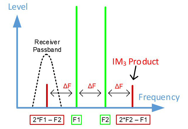
Figure 3 Two-tone receiver intermodulation test.
The two signals represented by solid green traces at frequencies F1 and F2 are the only ones applied to the receiver. The two signals represented by solid red traces are created inside the receiver passband and are processed by the receiver as external signals. The frequencies of the two red signals are 2F1-F2 and 2F2-F1, respectively and are known as intermodulation products of the third order.
With increasing levels of the two green signals, the two red signals increase significantly more due to nonlinear effects inside the receiver. When the levels of the two green signals are increased by 10 dB, for example, the internally created red signals increase, ideally, by 3 x 10 dB. In other words, the difference in level between the green and red signals is reduced by 20 dB for each 10 dB increase of the green ones. This enables a theoretical calculation of the level of the green interfering signals when the two red signals are at the same level.
This calculated level is called the intercept point third order (IP3) because with a further 1 dB increase of the green signals the red ones would then be 2 dB stronger than the green ones. The level for the IP3 is normally higher than the maximum allowed signal strength at a receiver’s front-end and should be seen as a reference value only to compare the intermodulation performance of different receivers. The IP3 value is also used to calculate the expected levels for internally generated red signals in the presence of external green interferer signals with given signal levels.
If the input IP3 (IIP3) of a single-stage amplifier measured with a two-tone signal is compared with its 1 dB compression point then the “exact” difference based on ideal mathematical models can be expected to be 9.6 dB.
In practice, the front-end of a receiver is built with a cascade of amplifiers and other stages, each with some nonlinear behavior. The combination of the individual characteristics of all components is responsible for an overall behavior that may differ from those of the single stages. For example, the overall 1 dB compression point of a receiver front-end may be the result of two amplifiers being compressed by 0.5 dB each, or some other combination.2
As a rule of thumb, the IP3 of a receiver, in practice, is typically 15 dB above a receiver’s 1 dB compression point, which is typically where another nonlinear effect called cross-modulation begins. Cross-modulation is a critical effect in systems where communication waveforms with amplitude changes or amplitude modulation are used. This is the case, for example, in systems used for air traffic control because the communication waveform used is a double sideband (DSB) amplitude modulation (AM) signal. The definition of the degree of cross-modulation is unfortunately not standardized and cannot be compared between different applications.
Cross-modulation occurs when a strong interferer drives the front-end into saturation. If an amplifier is saturated, its gain is reduced and any other low-level signal passing through the amplifier at the same time also sees some reduction of gain. As a result, the low-level signal is inverse-modulated by those parts of the interferer’s envelope that saturate the front-end (see Terms and Definitions)
An air traffic controller operating on a voice channel cross-modulated by another communication channel will not be able to communicate with pilots. Even a very high receive level will not help in this situation. The maximum operational limit of a receiver system is given by its cross-modulation threshold and not by any other parameters. If interferers are kept below the cross-modulation threshold, a receive system is basically operating within a linear area. Below this limit, reception quality is determined by key parameters of the receiver and those transmitters acting as interferers.
WHAT RECEIVER INTERMODULATION PERFORMANCE IS REQUIRED?
The relevant collocation scenario, which is the basis for the calculation of receiver parameters, is shown in Figure 1. This scenario is sufficient if only one transmitter signal acting as an interferer is present. If it is assumed that all stations involved are transceivers, then three stations are needed in total if a two-tone intermodulation calculation is done. The most important parameter for the derivation of receiver data from given transmitter data is an assumed antenna decoupling of 25 dB between the stations, which is a reasonable value for amateur radio contests and field days.
Figure 4 shows three transceiver stations, where two are transmitting while the third is receiving. The two transmitters operate at frequencies F1 and F2. The colors for the RF signals correspond to those used in Figure 3, but the sources and mechanisms for why these signals are present are different. Both transmitter signals with a power of 150 Watts (+ 52 dBm) each appear at a level of +27 dBm at the receiver’s input, which is consistent with the values in Table I.
The transmit signal of Transmitter 1 also appears with a level of +27 dBm at the antenna of Transmitter 2 because the antenna decoupling of 25 dB is valid for any combination of the antennas.
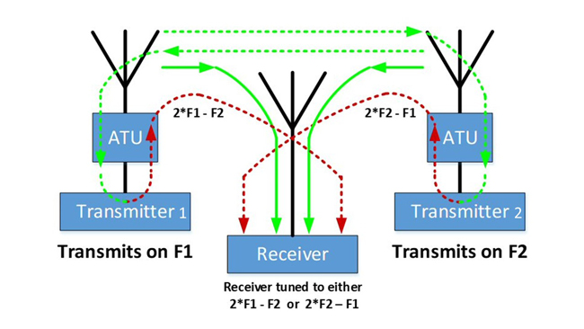
Figure 4 Two-tone interferer scenario.
This means that each transmitter is exposed to an interfering signal that is backward-radiated into its antenna. Based on a mechanism called “backward intermodulation” this transmitter creates a spurious signal that is then reradiated (see Figure 5).
The transmitter, which transmits on frequency F1 is exposed to a backward signal F2 radiated from Transmitter 2. As a rule of thumb, a modern transistor creates a new signal based on backward intermodulation effects which can be expected to be 30 dB lower than the level of the backward applied signal.
Within installations using antenna tuning units, the backward applied signal is attenuated by the selectivity of the antenna tuning unit in combination with the tuned antenna. The reradiated signal is suppressed even more because both signals appear at frequency offsets from the transmitter’s own transmit frequency. Figure 5 shows the worst-case scenario without antenna tuning units when broadband antennas are used.
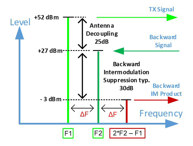
Figure 5 Spectrum at one of the transmit antennas.
At the antenna of Transmitter 2, a similar spectrum is present which is symmetrically mirrored. The transmitted spectra from both transmitter antennas are radiated to the receiver’s antenna and overlap there. As a result, the total spectrum applied to the receive antenna already contains intermodulation signals at exactly those frequencies that would be created by the receiver if no backward intermodulation signals from the transmitters were present.
Figure 6 shows the involved spectral components and their levels, which are now used to calculate a hypothetical receiver IP3. This hypothetical IP3 represents receiver performance that would lead to the same intermodulation products if only the two transmit signals were applied.
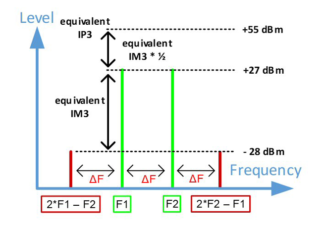
Figure 6 Spectrum at the receive antenna.
The two green lines represent the carrier levels of the two 150 Watt (+52 dBm) transmitters with an antenna decoupling of 25 dB to the receive antenna while the two red lines represent the backward intermodulation products of the two transmitters. The two backward intermodulation signals as shown in Figure 5 are also attenuated by the antenna decoupling of 25 dB and appear at a level of – 28 dBm at the receive antenna. Based on these parameters, a hypothetical receiver IP3 of +55 dBm is calculated, which is very high. These values show that it is quite unrealistic to operate a receiver at frequencies where intermodulation products may appear.2
FREQUENCY PLANNING INSTEAD OF VERY HIGH IP3
Within an operational scenario involving real transmitters, even an ideal receiver with extremely high intermodulation performance would not be able to use those frequencies for which intermodulation products may theoretically appear. The operational limits are set by the backward intermodulation performance of all involved transmitters creating signals on all potential intermodulation frequencies which are then applied to the receiver from outside.
The calculations show that all levels of intermodulation signals exceed the sensitivity threshold of a receiver by approximately 80 dB or more. For interference-free operation of those frequencies where intermodulation products may appear, both the involved transmitters and the receivers would need improvements by unrealistic orders of magnitude. This proves that the solution for interference-free operation is not a further improvement of either receiver or transmitter performance, but frequency planning.
The solution required must enable the operation of receivers and transmitters of different technologies and performance. Some large HF installations separate receiver and transmitter sites and build so-called “split site configurations” knowing that this is just a means to reduce the transmit signal levels and transmitter noise at all receiver front ends. However, this separation will not sufficiently reduce the intermodulation performance of the entire installation, because all transmitters (remaining close to each other) still create high-level backward intermodulation products at receiver locations. The question is, “How can intermodulation effects be overcome in practice?”
The only way to achieve interference-free operation is to establish a frequency planning method to avoid a situation where a receiver is tuned to a frequency where intermodulation products may theoretically appear. With large commercial stations like coastal sites or on Navy ships, frequency planning is standard using analytical tools. These tools are loaded with all frequencies that are candidates to be used and they calculate all permutations of frequencies in any combination of transmit and receive modes of all transceivers. They provide indications of potentially interfered frequencies and recommend optimized frequency channel allocations. Optimizations often prescribe just small frequency changes of some kHz for some transceivers, which puts all intermodulation products sufficiently outside a receiver’s passband.
A commercial site has all communication equipment within an installation under its control, and can, therefore, quite easily optimize the frequency plan. This situation is different for amateur radio events like field days, but frequency planning is also possible here as well if the operators are aware of the necessity.
The calculation of potentially interfered frequencies can be quite easily accomplished with a step-by-step approach if only the two strongest transmitter frequencies of all possible stations are considered. In this case, all involved frequencies are equidistant to each other for intermodulation of the third order. For intermodulation of the fifth order, the intermodulation products are double the distance from the two interferers.
In parallel and independent of that, it is recommended to operate two transmitters on two unfavorable frequencies just for test purposes to measure the intermodulation products by tuning a receiver to it. The measured levels help determine a suitable minimum required frequency shift, e.g. some kHz or more to bring the receivers into safe operation.
The calculation should be done for the operation of several amateur radio bands by different stations in parallel and for operation within the same band as well. For example, it may be that one station transmitter operates within the 10 m band and a second one operates within the 12 m band. By choosing unfavorable frequencies, in detail, intermodulation products may appear within the 15 m band. In this case, given equidistant frequencies relative to each other, a combination of one transmitter operated within the 12 m band with a second one within the 15 m band may lead to intermodulation products within the 10 m band. In this case, the introduction of a small frequency offset for one of these three stations of some kHz may be sufficient to achieve interference-free operation.
Intermodulation products within the same amateur radio band follow the same mechanism, but another significantly relevant difference in operational behavior is due to the low absolute frequency offset between the stations. In this case, it is likely that a small frequency shift will improve the intermodulation-related performance, but absolute performance will still suffer from strong transmitter noise or poor desensitization performance of the receiver. In this case, the limits as given in Tables I and II apply. After clarifying the operational context of intermodulation, no further receiver parameters need be added and the design of a transceiver architecture can begin using the parameters given in Tables I and II.
STARTING WITH THE TRANSMITTER RF CHAIN
The RF design for a transmitter can be simply seen as an RF signal generator with some amplifiers that increase the low signal level of the generator to the required high output power at the antenna.
A high-end transmitter is characterized by very low unwanted emissions outside the transmit channel. These unwanted emissions are either discrete signals or are represented by a noise floor. Discrete spurs can be caused by a variety of effects such as internal coupling of clock signals into the RF path. Other causes for discrete spurs can be nonlinearities in the transmit path, mainly within the final power amplifier. But before discrete spurs can be minimized, the basic design of the transmitter must first deliver a low noise floor, otherwise, the radiated unwanted noise may already significantly interfere with adjacent channels.
The unwanted noise floor can be separated into two different areas, which also represent two different noise-creation mechanisms (see Figure 7). The first area is close to the carrier and is normally called phase noise while the second area is far from the carrier frequency and is called broadband noise.
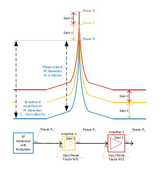
Figure 7 Total spectrum at the transmitter output.
While phase noise close to the carrier is defined by the quality of the RF generator, the broadband noise floor of the transmitter chain is mainly defined by the design of the amplifier chain behind the RF generator. Figure 7 shows where the spectrum delivered by the RF generator is simply lifted in level by two amplifiers.
For a high-end transmitter, the required broadband noise floor may be so low that even with an RF generator that produces no noise, the resulting noise floor after the amplifiers may be too high. This means that a significant improvement can only be achieved by inserting filters into the RF path. The optimization of this filter/amplifier chain must then be done by going backward from the antenna through all stages and analyzing the gain of each amplifier stage.
Figure 8 shows an improvement in the RF path by inserting two bandpass filters in front of each of the two amplifiers. The minimum broadband noise floor, which appears at the output of the transmitter, and the input to the antenna, is the noise present at the input of Amplifier 2, which is then increased by its gain.
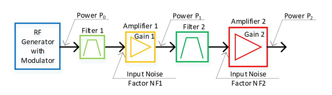
Figure 8 Improved transmitter RF path.
For a first optimization, the elements within the RF path can be seen as ideal, e.g. the filters do not have any insertion loss and the amplifiers have just an NF and a flat frequency response with a given gain. It is also assumed that a filter in front of an amplifier suppresses all broadband noise coming from previous stages completely. With this simplification, the broadband noise floor after the final amplifier is just the input noise floor represented by the amplifier NF, which is then increased by the amplifier gain.
While the output power of the RF generator inside the filters‘ passbands is increased by the amplifiers, the broadband noise floor outside the filters‘ passbands is first suppressed by the filters; then, a following amplifier just increases its input noise floor by its gain. Consequently, the output noise floor always remains quite low while the output power goes up by the total gain of the transmitter’s RF path.
In Figure 9, the dotted purple line shows broadband noise suppression by filters, which is then increased again by the following amplifiers. The most important parameters that define broadband noise performance at the antenna are the maximum allowed gain for each amplifier stage, which also determines the power levels appearing at the filters.

Figure 9 Spectrum of the improved transmitter RF path.
It may be that the filter in front of the final power amplifier must handle a power level of some Watts due to the quite low allowed maximum gain of the amplifier following it. Such a high-power filter may be difficult to realize, especially because it must be tunable in frequency as well.
On the receiver side, a similar high-power filter may be required to ensure sufficient receiver performance in the presence of strong interferers. Therefore, the dual use of relevant resources like filters and other components for the receive and transmit paths should be considered during the process of optimizing the overall RF transceiver architecture.
The RF Generator (Exciter) is the Heart of the Radio
The most important building block of a transceiver is the RF generator (see Figure 10). It provides a low phase-noise modulated RF signal that represents the complete transmit signal of the transceiver. It starts with a sufficiently high level providing an already low broadband noise as a starting point to the following filter/amplifier chain of the transmit path. In receive, the unmodulated RF signal is either used as a local oscillator for superheterodyne receivers or is used as a clock signal for digital direct sampling receivers.

Figure 10 Transceiver RF generator.
Today it is technologically possible to realize the core part of the RF generator, represented by the box with the blue dotted lines in Figure 10, with a fully integrated solution. Even digital-analog converters (DACs) can be part of such a chip. Only some manufacturers are currently providing fully integrated solutions, but with a split between purely RF functionality and the core direct digital synthesizer (DDS), a sufficiently higher number of components is available.
The information signal (e.g. voice or data) to be transmitted is filtered and adjusted in level and is then digitized. The digitized signal passes through a baseband processing stage that creates a digital I/Q signal stream representing the modulation, including filtering. This digital I/Q modulation information is complex multiplied with the digital unmodulated carrier signal from the numerically controlled oscillator (NCO). This fully I/Q modulated digital RF signal is then input to a DAC and appears at its output as an analog RF signal to be transmitted.
Smart Power Control Loop
It is recommended to use a configuration for the RF generator where two parallel outputs are available, one with the modulated RF transmit signal and one with the unmodulated RF signal derived from the same digital oscillator. This second unmodulated signal is used to supply a feedback path for phase-coherent demodulation of the RF signal after the final power amplifier.
If this feedback signal is also provided, an I/Q data stream with the same format as the modulation stream, then an easy vectorial comparison of these two signals can be done. The comparison is first used to set up a power regulation loop by monitoring the level of the transmit signal. A second comparison checks the quality of the transmitted signal by comparing the I/Q constellation diagram of the transmit signal with the feedback signal. Active linearization can be used to pre-distort the transmit signal, compensating for all influences on the way to the antenna through all stages.
The block diagram of a high-end transmitter illustrating this optimized transmitter path is shown in Figure 11. The key element is still the RF generator as shown in Figure 10; however, the RF generator is now enhanced with an additional block providing the power regulation loop including an active linearization capability. The required feedback path and all associated signals are shown in purple, while the normal transmit path is shown in blue.

Figure 11 Optimized transmitter RF path.
The feedback demodulator is connected to the forward output of a directional coupler between the final amplifier and the antenna. If a second feedback demodulator is connected to the reflected output of the same directional coupler a highly capable analysis of all signal signals traveling from the antenna back to the final amplifier can be done. Due to the phase-coherent nature of the demodulation, it is now straightforward to distinguish between signals that are reflections of the transmit signal and those that have been received by the transmit antenna from other transmitters.
Signals from other transmitters are characterized by a frequency offset as compared to the transmit signal and can now be isolated. This enables an optimized strategy, keeping the transmit power constant or reducing it not more than necessary, independent of the source of the reflected signals.2
Always Design the Power Amplifier (PA) for Good Linearity
Active linearization is a regulation loop that compensates for the effects of nonlinearities of all elements between the RF generator and the antenna. It must be carefully designed with respect to its bandwidth otherwise it may increase the phase noise outside its bandwidth where broadband noise starts. Even when having such a capability available in a transmitter path, any amplifier should always be designed to provide good basic linearity.
Nonlinearities of amplifiers can be based on a variety of mechanisms and are often described with very complex formulas in the literature, but the practical view describing nonlinearities is much simpler. If, for example, a digitally modulated single carrier is used as a transmit signal, then linearity is just how fast and how accurate the output signal of an amplifier can follow the input signal in phase and amplitude.
Figure 12 shows a typical digitally modulated signal, like quadrature phase shift keying (QPSK). Within this simplified view it is easy to see what happens if an amplifier has no problem following phase changes of the modulation signal (shown in the blue circle) but does have a problem following amplitude changes (shown as red arrow). It may be that a basically linear Class AB amplifier appears to be nonlinear, but the real reason for this behavior is that the amplitude changes within the modulation signal are faster than the AM frequency response of the amplifier.

Figure 12 Phase and amplitude changes after an amplifier.
The AM frequency response of an amplifier is a major parameter in the context of nonlinearities and is set and limited in most cases by the circuitry of the input stages and not by the transistor. For a Class AB amplifier, the gate voltage may increase with an increasing RF drive signal and opens the transistor for a higher output power. This leads to a dynamic shift of bias toward Class A. It is important here that the average DC bias voltage at the gate follows the average level of the drive signal fast enough, otherwise, the output power of the transistor cannot follow amplitude changes at the input fast enough. Figure 13 shows a simplified circuit of a push-pull amplifier that may limit the AM frequency response.

Figure 13 Input circuit limiting AM frequency response.
The incoming signal is changed from unsymmetric to symmetric by the balanced-to- unbalanced (BALUN) device and relative to GND, one transistor is driven with the positive half of the RF carrier sinewave while the second transistor is driven with the negative half and vice versa. The envelope of the modulation signal represents the level of the RF carrier and should look identical on both gates. The average instantaneous level of the envelope is responsible for opening the gate to the required source gate voltage, shown as dotted lines in Figure 13.
The elements C1/C2 and R1/R2 set a low-pass characteristic. If the time constants are set too low, then the average DC voltage of fast modulation peaks cannot follow the fast changes of the envelope. Consequently, the gates are supplied with gate voltages that are too low (shown as red dotted lines) during fast modulation periods while the RF envelope reaches full amplitude.
This leads to the suppression of fast amplitude changes in the signals, which looks like amplifier saturation. This mechanism creates almost the same intermodulation distortion as a saturated amplifier, but it is simply caused by a bandwidth limitation of the DC paths within the input circuits of the PA.
The behavior of an amplifier with a limited AM frequency response may lead to an eye diagram showing strong inter-symbol interference (ISI) with memory effects in the time domain. Figure 14 shows an example of an eye diagram of a binary phase shift keyed (BPSK) signal when AM bandwidth limitation occurs.
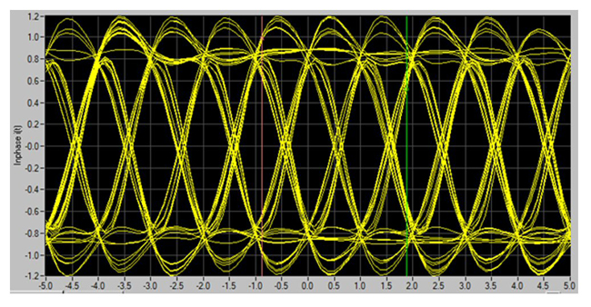
Figure 14 ICI caused by insufficient AM bandwidth.
ISI with memory effects may motivate some design engineers to compensate by using an active feedback loop implementing complex mathematical algorithms like the Volterra series and using a harmonic balance simulator for verification. It is therefore recommended to first optimize the AM frequency response of a PA according to the required bandwidth of the transmit signal and use the feedback loop for further optimization of the remaining nonlinear behavior if necessary.
The remaining signal distortion on the way to very high linearity may be complicated, like thermal effects which will then require complex mathematical solutions. In most cases, however, the linearity of an amplifier will be suitable for typical communication signals if the AM/FM frequency response is sufficiently high.
It is further recommended to design an amplifier for an AM/FM frequency bandwidth response that is at least two or three times higher than the highest modulation frequency of the signal to be transmitted. For an HF amplifier and SSB voice modulation, the AM frequency response should be at least 6 to 9 kHz. This method of improving the linearity of an amplifier is easily achieved and is easy to validate because only an AM signal is required for testing.
In a push-pull configuration, it is additionally important that the gates of both transistors see identical circuitry. In Figure 13, a DC path through the matching network connects the gates to both capacitors C3 and C4. It is likely that these capacitors have different values because they have been selected based on different goals; additionally, C4 is connected to a series impedance while C3 is directly connected to GND. As a result, the AM frequency responses at the two gates may be different from each other due to different capacitive loads. This leads to an unequal drive of the transistors. The circuitry can, therefore, not only ensure a sufficiently high AM frequency response but also an identical characteristic for each transistor.
With a good basic PA design, in combination with linearization, the following two-tone intermodulation values can be expected if the transmitter is driven with a two-tone signal leveled 6 dB below PEP for each tone. The IM3 values represent the difference between the intermodulation products and the two tones.
•IM3 ≥ 30 dB – basic linearity
•IM3 ≥ 40 dB – enhanced linearity using digital predistortion
•IM3 ≥ 45 dB – superior linearity using digital active linearization
Carefully designed in-band linearity of the transmitter chain enables good signal quality with respect to bit error rate (BER) or in-band signal-to-noise ratio (SNR). But even with very high linearity, beyond high-end requirements, some spectral regrowth may occur outside the transmission channel.
As a rule of thumb, the adjacent channel power (ACP) of a complex modulated single carrier waveform is typically lower than the in-channel power by the number of dBs expressed by the two-tone IM3. The out-of-channel spectral components will decrease in the same way as higher-order two-tone intermodulation products do.
When using an active linearization loop some instability may occur depending upon the antenna VSWR. Therefore, careful selection of the feedback loop operational parameters is essential, which normally results in a slightly reduced linearization capability in favor of higher stability.
HELPFUL DIFFERENCES BETWEEN HF AND UHF
A broadband transceiver can cover a wide frequency range, which may span from HF up to UHF at 600 MHz or more. It is helpful to divide this frequency range into sub-bands. The differences between these sub-bands are, ideally, distinguished by different operational uses. These differences may enable opportunities to adapt key parameters of the transceiver architecture to perfectly match the operational requirements and facilitate transceiver architecture simplifications as well.
For example, the operational use of the HF Band normally requires a significantly higher output power than typically required for operation within the UHF Band (e.g., between 225 and 400 MHz). The split into sub-bands opens some room for optimization and simplification of the transceiver architecture while important key parameters can always be kept optimum. Such a split helps not only with the selection of the best, most suitable, components, but it also reduces the relative bandwidth required for key components like couplers, combiners and matching networks.
On the transmitter side, the design of an ultra-wideband amplifier may combine an HF amplifier using e.g., high-power HF/VHF transistors with a UHF amplifier using UHF/SHF transistors. Additionally, within the HF Band, antenna tuning units are often required to enable the use of a variety of antennas. These antenna tuning units must be included in the design of a transceiver because their selectivity provides help with respect to transmitter spectrum shaping as well as receiver robustness.
On the receive side, an HF receiver (independent of whether it employs direct sampling or IF sampling) may be used as an IF receiver after VHF/UHF down-conversion as part of an overall superheterodyne concept.
The split into sub-bands makes sense for components close to the antenna but is probably not required for other building blocks (e.g., signal generation). For an RF generator, it is possible today to create highly linear signals with low phase noise up-conversion to very high frequencies, and a split into sub-bands will not provide any advantage.
SHARING RESOURCES BETWEEN TX AND RX PATHS
In the co-site scenarios, as previously described, two identical transceivers were used to find the best operating point with respect to antenna decoupling, transmitter noise and interferer level at the receiver input. With a very low-noise transmit signal, antenna decoupling to a receiver can be quite low and the receiver will still not see any relevant desensitization due to transmitter noise, although the resulting interferer level may be very high.
A very low-noise transmitter may not be allowed to come close to a receiver front-end with a low robustness or a noisy transmit amplifier may not be allowed to come close to a very robust receiver without losing receiver performance.
The combination of minimum antenna decoupling, maximum allowed interferer level at the receiver input and required transmitter noise can be optimized. This will lead to the best overall system performance. A goal for the designer of a transceiver RF path is for the robustness of the receiver to match the noise performance of the transmitted signal with a given antenna decoupling. It will lead to equal contributions based on transmitter noise and those based on receiver effects if the antenna decoupling is decreased and reaches a minimum allowed operational limit.
As a result of perfect harmonization, the co-site filters within the transmit RF path are operated at the same power level as the pre-selector filters in the receiver RF path during the presence of strong interferers. With harmonized characteristics of the filters, it is possible to use them not only within the transmit path but also within the receive path by inserting an RF switch to employ the filters either as pre-selectors in the receive mode or as noise reduction filters in the transmit path (see Figure 15).
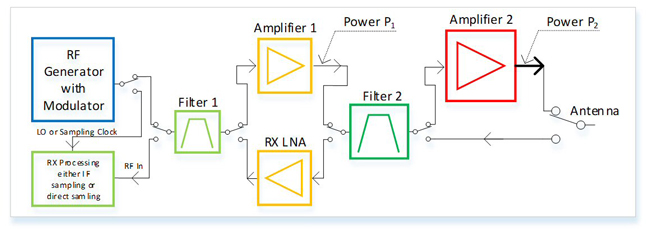
Figure 15 Resources shared between RX and TX.
The RF generator block is also shared. It delivers a high-quality low-noise noise-modulated signal for the transmit chain, and in the receive mode, it provides a local oscillator or clock signal to the receiver, either a superheterodyne concept or direct sampling.
CONCLUSION
A transceiver architecture comprises circuits for transmit and receive that can be designed to be completely independent from each other. An important step in optimization is to harmonize key parameters of the TX path with those of the RX path for best system performance with respect to co-location with low TX/RX antenna decoupling.
Harmonization of the RX path with the TX path within the transceiver architecture is then the basis for sharing valuable resources between these two parts. These shared resources may be high-quality filters that act as pre-selectors for the RX path or as co-site filters to reduce the noise of the TX path. Another sharable resource is the low-noise signal generator providing a clean transmit signal in the transmit mode which is also used as clean sampling, or mixing signal, in the receive mode for best desensitization performance. These steps can be the enablers for a compact and cost-effective design of a modern transceiver to provide excellent operational performance.
In the end, unit costs significantly influence the final architecture of a radio communication system and its components. For high-end installations (see Figure 16), such as military communication sites, radios can be adapted to the co-site situation. These radios can be equipped with special co-site options like hopping filters that are not only operated as pre-selectors for enhanced receiver robustness but are also reused as bandpass filters within the transmit chain as already shown in Figure 15.

Figure 16 High-end configurable V/UHF software-defined radio (SDR).
The co-site filters are active in all operational modes including fast frequency hopping. These special communication modes with hopping rates beyond 1,000 hops per second ensure a highly robust communication link even in the presence of intentional jamming signals. Superb RF specifications enable operation in complex antenna systems with antenna decoupling values as low as 25 dB (see Figure 17).
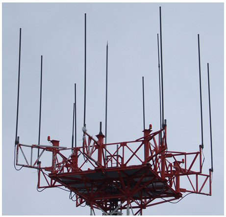
Figure 17 Complex antenna system with low decoupling.
For operation in such systems, the transmitters can be equipped with optional circulators to reduce transmitter backward intermodulation effects (see Figure 4) and, in combination with proper frequency planning as previously described, spurious free operation can be achieved.
TERMS AND DEFINITIONS
Cross-Modulation
Cross-modulation is an effect in which AM from a strong undesired signal is transferred to a weaker desired signal. Testing is usually done (in HF receivers) with a 20 kHz spacing between the desired and undesired signals, a 3 kHz IF bandwidth on the receiver, and the desired signal set to 1,000 μV EMF (-53 dBm). The undesired signal (20 kHz away) is amplitude-modulated to the 30 percent level. This undesired AM signal is increased in strength until an unwanted AM output 20 dB below the desired signal is produced.
A cross-modulation specification > 100 dB would be considered decent performance. This figure is often not given for modern HF receivers, but if the receiver has a good third-order intercept point, it is likely to also have good cross-modulation performance.
Cross-modulation is also said to occur naturally, especially in transpolar and North Atlantic radio paths where the effects of the aurora are strong. According to one (possibly apocryphal) legend, there was something called the “Radio Luxembourg Effect” discovered in the 1930s. Modulation from a very strong broadcaster (BBC) appeared on the Radio Luxembourg signal received in North America. This effect was said to be an ionospheric cross-modulation phenomenon. apparently occurring when the strong station is within 175 miles of the great circle path between the desired station and the receiver site.3, 4
Adjacent Channel Power Ratio
ACPR is an important performance metric used to characterize spectral regrowth in a transmitter front-end component or the entire chain. One of the main sources of spectral regrowth is PA nonlinearity. Therefore, this metric is often used to quantify the nonlinearity of a PA. It is also called adjacent channel leakage ratio (ACLR).
Inter-Symbol Interference
ISI is an effect where some energy of a modulation symbol also appears in other symbols and leads to interference. In the time domain it, looks like the symbols appear longer and are still present after the normal symbol time interval. This can be caused by propagation effects in the radio channel, but it may also be caused by nonlinear mechanisms within a transmitter’s PA. A receiver faced with ISI may not be able to clearly identify each symbol, which then leads to bit errors.
ACKNOWLEDGMENT
The authors would like to thank Manfred Fleischmann (Rohde & Schwarz), Robert Traeger (Rohde & Schwarz) and Harald Wickenhäuser (DK1OP, Rohde & Schwarz) for their support in the creation of this article.
References
- U. L. Rohde and T. Boegl, “The Perfect HF Receiver. What would it look Like Today?” Microwave Journal, Vol. 65, No. 5, May 2022, pp. 68-82.
- H. L. Hartnagel, R. Quay, U. L. Rohde and M. Rudolph, Fundamentals of RF and Microwave Techniques and Technologies, Chapter 9.6, Springer, 2023.
- J. Carr, The Technician´s EMI Handbook, Clues and Solutions, 1st Edition, Newnes, 2000.
- J. C. Pedro and N. B. Carvalho, Intermodulation Distortion in Microwave and Wireless Circuits, Artech House, 2003
For Further Reading
- U. L. Rohde, J. C. Whitaker and H. Zahnd, Communications Receivers: Principles and Design, McGraw Hill, Fourth Edition, 2017.
- ARRL. Web. https://www.arrl.org/.
- A. Farson (VA7OJ/AB4OJ), “A new Look at SDR Testing,” presented at the SDR Academy, 2016, Friedrichshafen, Germany.
- M. Fleischmann, A Novel Technique to Improve the Spurious-Free Dynamic Range of Digital Spectrum Monitoring Receivers, Dissertation, Brandenburgische Technische Universität Cottbus-Senftenberg, 2022.
- T. Boegl, “Test and Measurement for Radio Communication Equipment,” Rohde & Schwarz 2019.
- U. L. Rohde and M. Rudolph, RF/Microwave Circuit Design for Wireless Applications, Wiley, Second Edition, 2012.
- U. L. Rohde, Theory of Intermodulation and Reciprocal Mixing, Practice, Definitions and Measurements in Devices and Systems, Part 1, Synergy Microwave Corporation, 2001.
- P. Denisowski (KO4LZ), The Rebirth of HF, White Paper, Rohde & Schwarz North America. Web. https://www.rohde-schwarz.com/us/knowledge-center/videos/webinar-the-rebirth-of-hf-video-detailpage_251220-908608.html.