

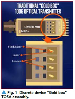
Optoelectronic industry designers have traditionally used discrete optical devices for transceiver designs. The process requires manual integration of discrete free-space optical components such as lasers, modulator, photo detectors, isolators, MUX/DE-MUX, lenses in the form of optical gold box sub-assemblies such as transmit optical sub-assembly (TOSA) (see Figure 1) and receive optical subassembly (ROSA). The TOSA and ROSA assembly process is quite restrictive and expensive because it may require multiple active and passive optical alignments during manufacturing e.g., laser to modulator, modulator to optical multiplexer, and de-multiplexer to photodiode etc., which makes the entire assembly process quite cumbersome. Due to the manual nature of the assembly process, it limits high volume manufacturing and the product ramp is usually difficult.
Until the last few years, silicon photonics (SiPh) technology was confined to the research lab, but it is now emerging as a mature technology. Many companies are able to successfully create SiPh products at a very competitive price point.
There is a paradigm shift in the industry regarding this new scalable technology, as it is showing rapid exponential growth and meeting the promise of high volume manufacturing. SiPh uses silicon as a medium for optical signal transmission. The major advantages of SiPh are the potential to integrate optical and electronic devices within the same IC and its compatibility with the existing complementary metal-oxide semiconductor process (CMOS) for fabrication.
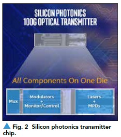
SiPh integrates a laser source, couplers, power dividers, modulators, optical multiplexer/demultiplexers, phase rotators, and attenuators giving a designer the ability to create the entire transmit and receive optical system within a single IC (see Figure 2). The number of assembly steps are dramatically reduced with SiPh devices and, therefore, so is manufacturing time and production cost.
Within a photonics IC, silicon waveguide is the most basic physical structure that guides the electromagnetic wave (light) from its input to output. The use of silicon waveguide for optical ignal transmission became feasible due to the high index contrast between silicon core and silicon dioxide cladding. Various types of optical waveguide designs are possible such as strip waveguide, rib waveguide, slab waveguide, and photonic crystal waveguide.
The fundamental principle in all these types of waveguide remains the same, but their geometry differs. Total internal reflection occurs when a high refractive index material (core) is surrounded by a low refractive index material creating a strip of high dielectric constant material, such as silicon, surrounded by a low dielectric constant material such as SiO2 and/or air. Figure 3 shows the electric field distribution across the cross-section of a strip waveguide. Optical confinement in the silicon on insulator (SOI) substrate allows tight bending of optical waveguides, thus ensuring high density integration of photonics devices.

In an advanced SiPh process, indium phosphide and germanium can be monolithically integrated on an SOI wafer to create integrated lasers and photo detectors. An important property of the SiPh device is the interactions between electrons and photons. The electrical signal can be converted to an optical one, and vice versa, by integrating lasers, modulators, and a photodetector.
The amplitude and phase of the optical signal can be manipulated by applying an electrical signal to an inbuilt semiconductor PN junction to create components like attenuators, phase shifters, and modulators. Two types of modulators are commonly used for data communication
applications: a travelling wave modulator and ring resonator modulator.
The travelling wave modulator is based on the Mach-Zehnder Interferometer (MZI) principle, where a collimated beam of light is split into two propagating waves which traverse through different optical paths and are recombined at the output using a second beam splitter/combiner. The intensity modulation will occur at the output of the beam combiner depending upon the relative phase shift acquired between the two optical paths. Constructive interference will occur if the two beams arrive with the same phase, and destructive interference will occur if the two beams are 180° out of phase.
In a travelling wave modulator (see Figure 4), the electrical-to-optical signal conversion is achieved by creating a semiconductor PN junction along the length of the optical waveguides. The PN junction and RF transmission lines form the travelling wave structure of the modulator. The travelling wave structure must be designed in order to match the phase velocity of the electrical signal propagating along the PN junction electrode with the phase velocity of the optical signal propagating along the optical waveguide. The modulating electrical signal is applied across the PN junction diode, which results in the refractive index change surrounding the PN junction and hence controls the phase shift of the optical signal. The length of the PN junction is chosen to provide a relative phase shift of 180° for the peak electrical signal, producing maximum intensity modulation. Both carrier injection or depletion types of PN junction designs are feasible, depending upon the design requirements.

A travelling wave modulator can be used for both NRZ and PAM4 signaling. These modulators tend to be a few millimeters long in order to achieve the required phase shift and require much higher drive voltage as compared to ring modulators.
The second type of modulator widely used in silicon photonics is the ring modulator. Ring modulators have become popular due to their ultra-compact size and low voltage swing requirements. Ring modulators consist of an optical ring resonator structure and an electrical PN junction surrounding the ring (see Figure 5). The ring resonator subcomponents include a directional coupler, a straight optical waveguide section (called a bus waveguide), and an optical feedback loop connecting one arm of the directional coupler from its output to the input in the form of a circular ring.

The CW laser source is connected to the input of the bus waveguide. The ring resonator dimension is optimized to provide resonance at the desired optical frequency. At the resonance frequency, a portion of the input optical signal gets coupled to the ring resonator, which travels around the ring repeatedly.
Every time this light signal travels around the ring, it accumulates a phase shift which amounts to an integer multiple of 2*PI. Subsequent wave front coupling from the bus waveguide will result in a constructive interference within the ring, producing resonant effects. Due to this resonance, the transmission spectrum at the output of the bus waveguide will show a strong dip. One can consider a ring resonator as a narrowband frequency or wavelength domain notch filter. The ring modulators are designed to carefully position the operating wavelength on the slope of the resonance peak so that a slight shift in the resonance will show up as intensity modulation at the output of the bus waveguide. A highfrequency electrical signal across the PN junction will change the refractive index and cause a shift in the resonance peak, producing desirable intensity modulation at the output of bus waveguide.
Ring modulators have small optical bandwidths and are quite sensitive to fabrication tolerance, thermal characteristics, and operating conditions. So, a stabilization and thermal control circuit is required to operate the ring modulator. They can also be used for both NRZ and PAM4 signalling.
The current state of pluggable transceiver technology provides a maximum of 400 Gbps data throughput. Products such as 400G DDQSFP and OSFP are available now for data center applications. For example, a 400G product uses PAM4 signaling with eight channels running at 50 Gbps per channel
for the host-side transmission, while four channels at 100 Gbps handle the line-side transmission.
A 400G DR4 product is based on a single wavelength, four pair of parallel fiber, while FR4 is based on wavelength division multiplexing/de-multiplexing within a SiPh chip enabling 400G transmission on a single pair of fiber. Hyper-scale datacenters (HSDC) typically require up to 1.5 million optical
transceivers, creating a huge demand for 100G/400G products. The exponential growth in data communications supported by HSDC is due to AR, VR, VOD, 5G, IoT, and autonomous driving, applications that are dictating much higher bandwidth and lower power consumption for future products.
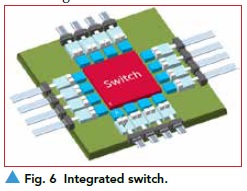
Next-generation products, such as an 800 Gbps/1.6 Tbps link will require eight/16 lanes running at 100 Gbps per channel for host-side transmission, severely limiting the pluggable transceiver applications due to speed, power, and thermal constraints. This will create a huge opportunity for silicon
photonics integrated solutions (see Figure 6). Tight integration of 16 or more channels to achieve 1.6 Tb or higher data throughput per device will bring integrated silicon photonics close to the ASIC, avoiding the need of re-timers on the host board. These highly integrated SiPh solutions will allow us to
address high bandwidth, power, and thermal requirements for any future products that would be quite difficult if not impossible to meet using traditional discrete optical devices.
Article was published in the SIJ July 2019 Print Issue, Fundamentals: Page 48.
For More Information
1. L. Chrostowski and M. Hochberg, “Silicon Photonics Design: From Devices to Systems, First Edition.”
2. C. E. Png, S. T. Lim, T. Y. L. Ang, and J. R. Ong, “Silicon Modulators for 25 Gb/s Photonics Platform,” 2017 Conference on Lasers and Electro-Optics
Pacific Rim (CLEO-PR).
3. A. Samani, M. Chagnon, D. Patel, Q. Zhong, S. Ghosh, M. Osman, D. V. Plant, and V. Veerasubramanian, “A Low-Voltage 35-GHz Silicon Photonic Modulator-Enabled 112-Gb/s Transmission System,” IEEE Photonic Journal, Vol. 7, No. 3, June 2015.
4. M. C. Tien, “SIlicon Photonic Devices for Optoelectronic Integrated Circuits,” Electrical Engineering and Computer Sciences, University of California at Berkeley, Technical Report No. UCB/EECS-2009-118.
5. W. Bogaerts, P. De Heyn, T. Van Vaerenbergh, K. De Vos, S. Kumar Selvaraja, T. Claes, P. Dumon, P. Bienstman, D. Van Thourhout, and R. Baets, “Silicon Microring Resonators,” Laser Photonics Rev. 6, No. 1, 2012, pp. 47–73.
6. Lumerical Interconnect User Manual.