
Printed circuit boards (PCBs) designed for radar and military communication applications are complex and must adhere to strict IPC standards. They must undergo rigorous testing to ensure their reliability and stable performance under demanding conditions. These boards operate at radio frequencies, so maintaining good signal integrity is crucial. Perfecting high frequency board designs often requires multiple iterations, which are expensive and time-consuming. The best way to tackle this challenge is to identify and resolve potential manufacturing issues through design-for-manufacturing (DFM) analysis. The standard DFM checks include trace and drill spacing, pad size and solder mask clearances. But in RF boards, you must also consider the probability of issues arising from hybrid stack-up, antennas, ground-stitching, differential pairs and controlled impedance.
DFM Analysis Process
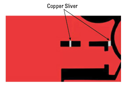
Figure 1 Copper slivers in a PCB design.
During the quote process, PCB designers determine the expected deliverables, testing requirements and comprehensive production documentation that will be sent to the contract manufacturer. Once the required data is received, DFM analysis is conducted at the fab house. After checking the production files for missing data, a tool number is assigned to the project. Next, the CAM team runs design rule checking (DRC) to identify any design errors. They ensure that all the design specifications align with their capabilities. For example, they check if the desired microvia aspect ratio is achievable. CAM engineers will also identify potential DFM issues that DRC may overlook, such as copper or solder sliver formation, as shown in Figure 1.
During DFM analysis, the manufacturer will conduct an in-depth board layout analysis, adding or removing features to increase the yield. For instance, a copper thieving pattern is added to an empty space on signal layers to avoid plating or etching issues. Snapshots of all the errors and required modifications are documented in a DFM report and sent to the customer/designer. After the designer’s approval, the fab house proceeds with the manufacturing process.
Essential DFM Factors of Radar and Military Communication PCBs
Design Files for Class 3 Boards
Conveying precise design specifications to your PCB manufacturer is crucial for military-grade PCBs. The fabrication drawing should include a board outline with dimensions, stack-up details, a drill chart and fab notes.
Clearly define the following in your fabrication notes:
- IPC Class 3 or MIL-PRF-31032 standard requirements
- Material details with UL ratings, Tg and RoHS compliance
- Manufacturing tolerances
- Presence of via-in-pad and buried or blind vias
- Via plating and filling details (e.g., Type VII filling as per IPC 4761)
- Controlled impedance with impedance value, trace width, layer number and type of trace (single-ended or differential pair)
- Solder mask color and surface finish
- Types of tests and their standards (e.g., IPC-TM-650).
After downloading the production documentation, ensure that no data is missing and that all the files are in the required format:
- Artwork data: IPC-2581, ODB ++ or Gerber 274X
- Embedded aperture information: IPC-2581, ODB ++ or Gerber 274X
- Netlist in IPC-356 format
- N/C drill and route data: Excellon or Plotter format
- Fabrication drawings: HPGL, AutoCAD, PDF or Postscript
- Pick and place file: CSV, text or ASCII.
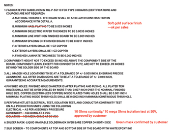
Figure 2 Sample of corrected fab notes after DFM analysis.
Choose a file format compatible with your manufacturer’s system. The manufacturer will contact you if any modifications are needed in your design. Figure 2 shows an example of a CAM engineer suggesting changes to the customer’s fab notes after performing a DFM analysis.