
Dielectric Material For Military-Grade PCB Designs
Military-grade PCBs are expected to provide high-level, uninterrupted performance in extreme environments. Heat-resistant and high-quality materials are always preferred to ensure circuit board reliability. Choose the substrate listed under the qualified parts list (QPL) on the Defense Logistics Agency (DLA) database.1 These materials are tested and approved to meet specific military standards.
Radar and milcom PCBs usually operate at radio frequencies, so the material experiences substantial insertion losses. PTFE materials like Rogers Duroid and RO4350 B are commonly used as they exhibit low Dk, low loss tangent and consistent electrical characteristics over a wide range of frequencies. IPC-4103 defines standards for copper-clad, laminates and bond ply in high frequency applications.
The following material parameters are checked during the DFM analysis of radar or milcom PCBs:
- The chosen materials are listed under the QPL and meet the design’s thermal, mechanical and electrical requirements
- Dielectric constant and loss tangent are within the specified ranges for signal integrity and controlled impedance needs
- The thermal conductivity and coefficient of thermal expansion (CTE) are within the required range so that the materials can withstand thermal cycles and soldering processes without degrading
- The materials are compatible with the manufacturing processes, including lamination, drilling, plating and soldering
- The selected materials are readily available in the required quantities
- Whether they are compatible with HDI and fine-pitch components if present in the design.
Note that PTFE materials need different drilling methods, hole treatment (plasma etch) and etching processes due to their fragile and non-stick properties. This will eventually increase the manufacturing cost. Always consult your fab house before choosing the material.
Hybrid Stack-Up
A hybrid stack-up is built using a combination of mixed materials. By combining different substrates in different layer configurations, the circuit’s electrical properties can be tailored to specific needs. This customization allows for better signal integrity, impedance control and power distribution performance. It also reduces the production cost as the desired electrical characteristics can be achieved without relying solely on expensive materials.
Consequently, manufacturing a mixed-material stack-up is complex. If the expansion rates of the substrates differ, it causes registration issues and cracks in the stack-up. Adhesion properties vary between materials; hence, choosing a suitable bonding material is necessary to avoid delamination problems. The choice of material also affects the drilling rate, hole treatment and plating process.
Any stack-up error will cause the PCB to fail reliability tests like highly accelerated life test (HALT) and highly accelerated stress screening (HASS), which are usually conducted on military-grade PCBs. Hence, the manufacturer ensures the materials are compatible with matching CTEs and bonded with the appropriate materials during the DFM process. They also check the feasibility of building the stack-up with available equipment and established processes.
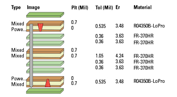
Figure 3 Example of a hybrid stack-up.
Figure 3 shows an example of a hybrid stack-up of Rogers 4350-LoPro and Isola 370HR. The build includes blind and buried vias with an overall board thickness of 0.065 in.
Controlled Impedance Traces and Differential Pairs
When performing DFM analysis for controlled impedance, the following parameters are considered:
- Trace width and spacing conform to the calculated values of the desired impedance
- Trace shapes (microstrip, stripline, coplanar waveguide) match the impedance requirements
- Line edges are smooth and free from irregularities
- Meandering is done at the appropriate section of the trace
- A continuous return path (ground plane) is beneath or alongside the traces
- Vias and pads do not disrupt the impedance
- Traces are isolated from noisy components, ground pours and guard traces
- Differential pair traces are length-matched within the specified tolerance to prevent skew
- Trace bends use appropriate radii to minimize impedance discontinuities.
Generally, the fab house modifies the trace width or dielectric spacing to achieve the desired impedance value. Before making the changes, the designer gives consent to the fab house. Figure 4 shows an example of matching the length of a differential pair of transmission lines.
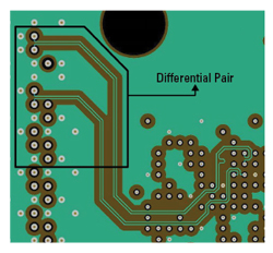
Figure 4 Differential pairs matched in length.
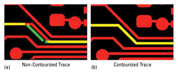
Figure 5 (a) CAM snapshot of non-contoured trace. (b) CAM snapshot of contoured trace.
Contouring Traces
In EDA tools, when a trace or pad is contoured, the entire feature will be locked and it can no longer be edited. This option should be used for oddly shaped traces and copper fill in your layout. Having features that are unnecessarily contoured does not create manufacturing issues, but it does hinder the DFM analysis. In addition, the CAM engineers cannot add test points to the contoured pads. To resolve the issue, they must individually add small pads to the test point, which increases the time required to complete the task. Figure 5a shows a non-contoured trace and Figure 5b shows the trace after contouring. It should be noted that all the features can be contoured if the design is created using AutoCAD and later converted into Gerber using CAM software.