
PCB Antenna
Whether to build it or buy it is a common dilemma every layout engineer faces when considering an RF PCB antenna design. Many factors, such as board quantity, layout, cost and available resources, come into play. Antenna design requires extensive knowledge, advanced design tools and simulation software. Designing an antenna is only feasible for mass production. For low quantity production or prototype volumes, purchasing an antenna may be the best choice. This build or buy decision is crucial as you must tailor your entire PCB design according to the antenna.
If you choose to design, consider the operating frequency, radiation patterns, gain, bandwidth and polarization. After designing, create and simulate a model antenna to verify its performance. Share the simulation results with your PCB manufacturer.
If the choice is to purchase, a designer must follow the exact specifications provided by the antenna OEM in the design and communicate these specifications to the PCB fabricator. The designer must also double-check the manufacturer name and the part number in the BOM. Monopole, printed dipole, patch, wire, ceramic and inverted F antennas are commonly used in circuit boards.
Key antenna design aspects checked during DFM analysis include:
- Board material and thickness
- Stack-up arrangement (usually, the region below the antenna should not have any components or conductors)
- Antenna position and orientation
- Clearance from the board edge
- Uniform impedance (matching impedance) between the antenna and the connecting trace
- Isolation from other nets and components.
Via Design
Multiple rules apply to vias and their pads in military-grade PCBs, which are prone to damage in extreme environments. According to IPC standards, burrs and stubs are not allowed in drilled holes. To avoid them, positive etch-back and back drilling procedures are typically used. Copper wrap plating for plated vias is mandatory to improve reliability because this procedure minimizes the possibility of cracks in the via-in-pad during thermal cycling.
If the filled vias are copper-plated, no voids should be exposed in the filling. However, bumps and dimples are allowed. The inner and outer annular rings should be a minimum of 0.001 in. and 0.002 in., respectively. Teardrops need to be added to the pads and the non-functional pads on the internal layers can be removed. This decreases unnecessary spacing issues and increases yield.
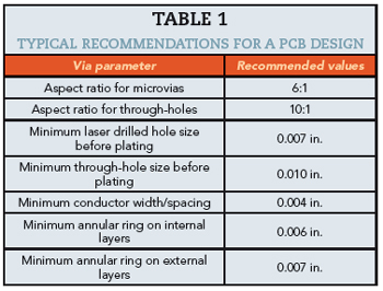
Table 1 shows the recommended values for common via parameters for a military-grade design. It should be noted that values can vary among different manufacturers.
All plated through-holes, pads and hole-to-pad ratios are examined in the DFM process to ensure that they comply with the capabilities of the fab house. The minimum drill size and final board thickness are checked to see if they meet the required aspect ratios. The design must allow modifications for tooling requirements. Some PCB suppliers offer PCB design tools to assist designers in building reliable boards. Sierra Circuits, as an example, offers Stack-Up Designer, Impedance Calculator, Material Selector, Better DFM and BOM Checker as free tools for circuit board design.
Ground-Stitching Vias
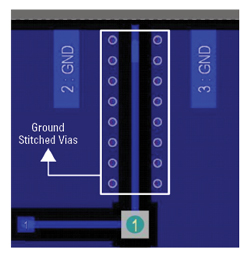
Figure 6 Ground-stitched vias placed across a coplanar trace.
Although it is not the norm, most RF designs have copper pours on the top and bottom layers stitched with vias to avoid EMI issues. This helps maintain a constant impedance in sensitive traces when they transit through different layers. Additionally, stitching vias can be used to connect a multi-ground plane design across multiple layers. Figure 6 shows an example of this technique with ground-stitched vias across a coplanar circuit trace.
For military applications, stitched vias can facilitate better heat dissipation, which can help them operate better in harsh environments. However, designing ground-stitched vias presents many challenges. These challenges include:
- The unintentional creation of copper islands on the inner layers of the board. If these are not identified and grounded, they will become floating copper and cause EMI issues.
- Insufficient spacing between the vias can lead to crosstalk and signal degradation. Maintaining a spacing of λ/10 for high frequency designs is recommended, where λ represents the signal’s operational wavelength.
- Holes too close to the board’s edge can get easily fractured, so keep a minimum clearance of 0.008 in. between the hole and the board’s edge.
- Less drill-to-copper clearance will cause signal integrity issues. Maintain a minimum drill-to-copper clearance of 0.008 in. for 8+ layer PCBs and 0.007 in. for 4-6 layer boards.
- Unplanned via placement can create hotspots instead of dissipating heat. So, place the vias strategically around the heat-generating components and traces.
All these clearances are double-checked during the DFM analysis to avoid issues during the manufacturing stages.
Surface Finish, Solder Mask and Silkscreen
Surface finish protects PCBs from contamination and chemical exposure. Hence, the IPC standard clearly defines the thickness, uniformity, coverage and solderability criteria for surface finish. The choice of surface finish and its thickness should be mentioned in the fab notes.
Recommended surface finishes for military-grade PCBs are:
- Electroless nickel immersion gold (ENIG)
- Soft gold
- Electroless palladium immersion gold (EPIG)
- Immersion silver.
IPC-6012 defines standards for solder resists:
- Copper features where a solder mask is required should not be exposed
- Edge board connectors, golden fingers and surface-mount lands should be free of solder masks
- Solder mask adhesion should be 100 percent for bare copper and laminates
- No voids are allowed if a solder mask is used to tent vias.
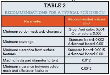
Recommended values for solder mask coverage and clearance parameters are shown in Table 2. Note that these values can vary among different manufacturers.
The silkscreen should be legible to facilitate the assembly process, repair and rework. The recommended minimum text height is 0.025 in. and the minimum line width is 0.004 in. The text must not overlap on adjacent pads or it might create solderability issues. A minimum 0.005 in. clearance should be provided between the silkscreen and other copper features.
Conclusion
PCBs for radar and milcom applications demand adherence to stringent IPC standards and meticulous attention to detail. The article has presented a number of factors, along with guidelines and recommended values for important considerations in the DFM process. By considering these factors and recommendations in a PCB design and closely collaborating with the fabricator, the number of iterations needed to achieve reliability and stable performance can be reduced and the process can be optimized.
REFERENCES
- Qualified Products Database or Qualified Products List, Defense Logistics Agency, Web: https://www.dla.mil/Working-With-DLA/Applications/Details/Article/2923127/qpdqpl-qualified-products-database-or-qualified-products-list/.