An improved Grey Wolf Optimization (IGWO) algorithm is described for the extraction of heterojunction bipolar transistor (HBT) small-signal model parameters. The IGWO algorithm balances its global and local search ability to minimize the error between modeled and measured S-parameters. The effectiveness of the method is verified by comparing modeled results with measured S-parameters of a 1×15 μm2 emitter-area InP HBT under two different bias conditions. Simulated S-parameters agree well with measured data over the frequency range of 0.1 to 40 GHz.
With the development of semiconductor manufacturing technology, the performance of InP HBTs have continuously improved, which makes it a promising device for microwave and mmWave applications.1-4 It is important for researchers to understand the physical structure and working mechanism of this semiconductor device, while the accuracy of the device small-signal model is key to optimizing circuit performance.5-7 Therefore, methods to extract accurate model parameters have attracted much attention.8-10
For HBT devices, the typical parameter extraction methods can be divided into direct extraction11-13 and numerical optimization.14 The direct extraction method must measure the device S-parameters under prescribed bias conditions many times. Then, the parameters of the equivalent circuit are gradually obtained by cumbersomely stripping off the parasitic parameters. The numerical optimization method minimizes errors between measured and modeled S-parameters by determining the order of magnitude of the parameters to obtain more accurate parameter values.
Alternatively, many researchers have tried a variety of optimization methods, such as genetic algorithms (GA),15,16 particle swarm optimization (PSO) algorithms,17 and differential evolution (DE).18 Although these methods can guarantee unique solutions, accuracy and convergence speed are still unsatisfactory when applied to the optimization of continuous functions.19,20
In recent years, some researchers have proposed swarm intelligence optimization algorithms such as the Whale Optimization Algorithm (WOA),21 Dragonfly Algorithm (DA)22 and Grey Wolf Optimization (GWO).23,24 GWO is an intelligent algorithm inspired by grey wolf group hierarchy and predation behavior of wolves as they track, surround, chase and attack their prey. It has the characteristics of a simple model structure, fast convergence speed and good optimization performance. However, similar to other swarm intelligence optimization algorithms, the GWO algorithm has the disadvantages of low solution accuracy and a tendency to converge prematurely.25,26
To coordinate the global and local search abilities of the GWO algorithm, a nonlinear dynamic convergence factor based on the tangent function is described in this work.
SMALL-SIGNAL MODEL
The adopted HBT small-signal equivalent circuit model is shown in Figure 1.11 Outside the dotted line in the figure are the parasitic and extrinsic parameters, where Cpbe is the base-emitter pad parasitic capacitance, Cpce is the collector-emitter pad parasitic capacitance and Cpbc is the base-collector pad parasitic capacitance. Lb, Lc and Le are the base, collector and emitter parasitic electrode inductances. Rb, Rc and Re are the base, collector and emitter parasitic resistances. Cbcx is the external capacitance of the base-collector junction. Among these parameters, only Cbcx varies with bias; the other parameters are bias-independent.
The dotted box in the figure contains the intrinsic parameters, including the intrinsic base resistance Rbi, dynamic base-emitter resistance Rbe, intrinsic base-emitter capacitance Cbe, intrinsic base-collector capacitance Cbc, intrinsic base-collector resistance Rbc, DC transconductance gm0 and delay time τ. These parameters are considered bias-dependent.5
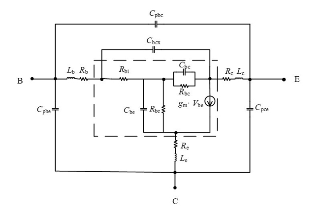
Figure 1 HBT small-signal equivalent circuit model.
SMALL-SIGNAL MODEL PARAMETER EXTRACTION
Extraction of Parasitic Parameters
1) Parasitic Capacitance Extraction
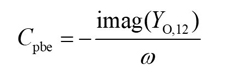
An open circuit test structure to extract parasitic pad capacitances (Cpbe, Cpce, Cpbc) is shown in Figure 2.27 The S-parameters of the measured open circuit test structure are converted to Y-parameters (YO), which are given by Equation (1).
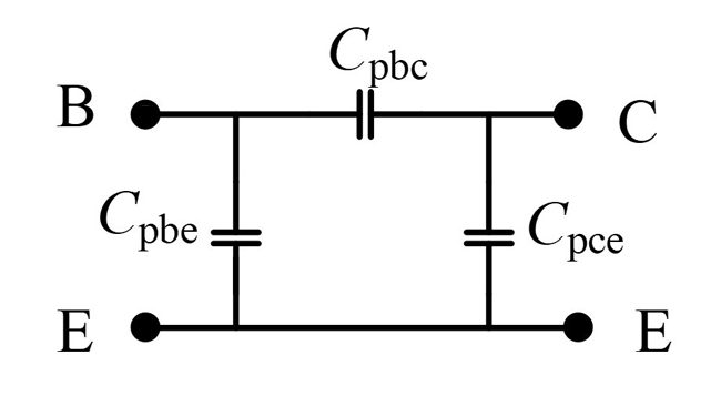
Figure 2 Open circuit test structure.

From Equation (1), it can be deduced that the related expressions of parasitic pad capacitances are expressed in Equations (2) through (4).


2) Parasitic Inductance Extraction
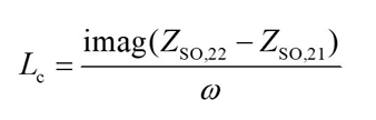
Figure 3 shows the short circuit test structure used to extract parasitic inductances. The influence of parasitic pad capacitances is removed before extracting the parasitic inductances. The S-parameters of the short circuit test structure are converted into Y-parameters, which are represented by YS. After eliminating the parasitic pad capacitances, the parasitic inductances are directly determined by using the Z-parameter (ZSO) matrix (see Equation (5)).
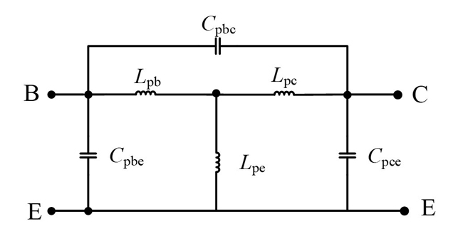
Figure 3 Short circuit test structure.

From Equation (5), the related expressions of parasitic pad inductances are shown in Equations (6) through (8).


3) Parasitic Resistance Extraction
Once the parasitic capacitances and inductances are de-embedded, the resultant part under the open collector condition, called EROC, is shown in Figure 4. The Z-parameters of EROC can be written as:28
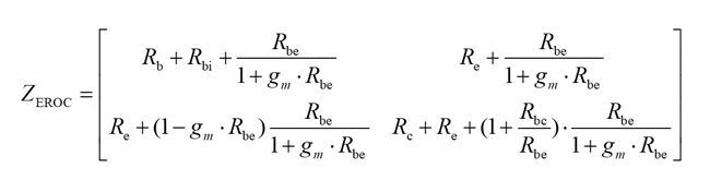
with


Where ηbe and ηbc are the ideality factors of the base-emitter and base-collect junctions, respectively, K is Boltzmann’s constant, T is the absolute temperature and q is the electronic charge. Ibe and Ibc are the DC currents flowing through the intrinsic base-emitter and the intrinsic base-collect junctions, respectively, which are proportional to the base injection current. When the base injection current is large, Rbi, Rbe and Rbc tend to zero. The parasitic resistances Rb, Re and Rc can be obtained from Equations (12) through (14).
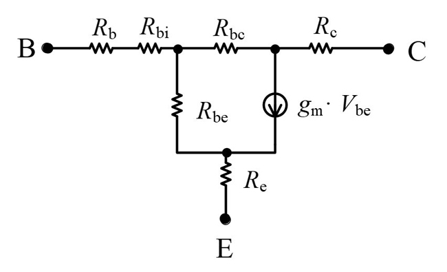
Figure 4 Open collector equivalent circuit.


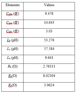
The values of the extracted parasitic parameters are listed in Table I.
TABLE I - EXTRACTED PARASITIC PARAMETER VALUES OF SMALL-SIGNAL MODEL