
An oscillator noise model distinguishes between various noise sources and predicts their influence on voltage-controlled oscillator (VCO) single sideband noise. Tuning diodes are the most critical elements. A test oscillator validates the predicted performance. An equivalent noisy resistor is introduced as a figure of merit for low noise diodes. Finally, the important fabrication considerations for low noise diodes are presented and validated in the test oscillator. At 10 kHz offset, the noise contribution of optimized tuning diodes in the oscillator adds only 10 dB of noise compared to a fixed capacitor design.

Figure 1 Generalized oscillator circuit using an amplifier model. ZL is the load.

Figure 2 Colpitts oscillator with base lead inductances, Lp, and package capacitance Cp.3, p. 132
Nearly all RF oscillators are voltage-controlled. The main single sideband noise contribution comes from the transistor’s intrinsic noise sources and the noise contribution of the tuning diode. The published flicker noise exponent (AF) and flicker noise coefficient (KF) values for transistors are usually determined at μV RF levels and normal DC operating conditions. As the RF level in an oscillator is much greater, this must be considered in the circuit analysis.
Most semiconductor companies changed their production processes for tuning diodes due to requirements of digital applications with the result that oscillator phase noise deteriorated. Also, none of the diode manufacturers specifies phase noise in oscillators, as there are too many variations of oscillator circuits available.
To develop and characterize low noise tuning diodes, it is necessary to describe the appropriate oscillator, analyze its critical semiconductor components and finally compare the tuning diode with the ideal case of a fixed capacitor. This article follows that guideline to verify the quality of newly developed tuning diodes.
ANALYSIS OF THREE-REACTANCE OSCILLATORS
A generalized circuit for an oscillator is shown in Figure 1. This is typically referred to as a Colpitts oscillator.1 It has a capacitive voltage divider, Z1 and Z2, and an inductor Z3. Its phase noise can be determined with a microwave simulator. With these programs, however, it is not possible to distinguish the individual noise contributions to the output signal. Therefore, a direct analysis of the oscillator circuit equations is presented here. The active device is a three-terminal device, typically a transistor.2
Figure 2 shows the Colpitts oscillator including leads and package parasitics. In practice, the lossy part of a tuned circuit is the inductor. Rs1 is the resonator loss. Splitting the input impedance ZIN (see Figure 1) of the Colpitts oscillator into real and imaginary parts we obtain:
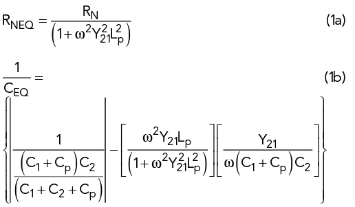
Where:
RN: Negative resistance without lead inductance and package capacitance
RNEQ: Negative resistance with base-lead inductance and package capacitance
CEQ: Equivalent capacitance with base-lead inductance and package capacitance.
The method shown is based on one-port oscillator design.3,4,5 The negative real part of ZIN compensates the resistor loss of the parallel tuned circuit.
Equation (1b) can be solved for CEQ, see equation (2a), imaginary part. The exact calculation of the “noisy” negative real part of the resistance ZIN, package, which is needed to compensate the tuned circuit loss, is given by:
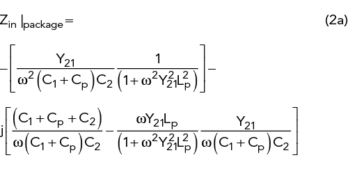
The left part is the negative part of the “noisy” input resistance. The intrinsic value RN is:
This is a noisy electronically generated negative resistance. It combines all internal noise sources to be modulated on the oscillator carrier frequency.
Leeson’s Empirical Phase Noise Model
E.J. Baghdady et al.6 first gave the definition of phase noise. Single sideband phase noise equation (3) is based on David Leeson,7 Scherer and Rohde.8 Scherer was the first to introduce the flicker effect to the Leeson equation and Rohde the first to add the AM-to-PM (VCO, last term in the equation) conversion effect, caused by the nonlinear capacitance of the active devices.
Leeson’s complete phase noise equation is given by:
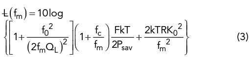
Where:
£(fm) = ratio of sideband power in 1 Hz bandwidth at fm to total power in dB
fm = frequency offset, or modulating frequency
f0 = center frequency
fc = flicker corner frequency
QL = loaded Q of the tuned circuit, should be half of the unloaded resonator Q0 (Matching for Power)
F = large signal noise factor
kT = 4.1 × 10²¹ at 300 [K] (room temperature)
Psav = average power at oscillator output
R = equivalent noise resistance of tuning diode (typically 200 [Ω] to 10 [kΩ])
K0 = oscillator voltage gain
k = Boltzmann constant.

Figure 3 Equivalent feedback models of oscillator phase noise.3,8

Equation (3) is shown graphically in Figure 3. The problem is that necessary data, like output power, large signal noise figure, loaded Q and flicker noise are not known a priori. The other problem is that it does not provide the actual noise contribution of the semiconductor devices. It is shown below that the phase noise contribution of the tuning diode in VCOs is the critical part, and not the transistor itself. The fixed frequency oscillator is the best phase noise case.
Depending on the relation between fc and f0/2QL, there are two cases of interest. For the low-Q case the spectral phase noise is unaffected by the Q of the resonator, but the £(fm) spectral density will show a 1/f3 and 1/f2 dependence close to the carrier. For the high Q case, a region of 1/f3 and 1/f should be observed near the carrier.
At small offset frequencies from the carrier, the phase noise exhibits a slope of 1⁄Δf3, i.e. 30 dB per decade. This region is dominated by flicker noise up-conversion. Particularly, in CMOS this is a challenge, since the 1/f-noise corner frequency is very high. Above that, the slope is 20 dB per decade. This is the offset frequency region dominated by thermal noise up-conversion. Finally, at higher offset frequencies from the carrier the spectrum is flat, limited by the noise floor of the active circuit (see Figure 2), given by kTF⁄Psig9 For very high Q resonators, the flicker corner frequency fc moves to higher frequencies, independent of the transistor (filter effect).
Table 1 shows fc as a function of the collector current IC for a typical small-signal microwave bipolar junction transistor (BJT). IC(max) of this transistor is about 10 mA. The corner frequency increases non-linearly with current (DC).
Note that fc, which is defined by AF and KF in the SPICE model, increases significantly with IC. This gives a clue about how fc changes when a transistor oscillates at different current levels. Because of the bias-point shift that occurs during oscillation, an oscillating BJT’s average IC is higher than its small-signal IC. KF is therefore higher for a given BJT operating as an oscillator than for the same transistor operating as a small-signal amplifier. Generally, fc varies with device type as follows: Si JFETs, 50 Hz and higher; microwave RF BJTs, 1 to 10 kHz (as above); MOSFETs, 10 to 100 kHz and GaAs FETs, 10 to 100 MHz.
Several observations can readily be made. One obvious way to reduce phase noise is to increase the power or oscillation amplitude. This, however, is limited in practical oscillators due to the supply level. Another, more practical, possibility is to increase the quality factor of the tank. The first part of equation (1), describing 1⁄Δω2, corresponds to the thermal noise part of the spectrum. Multiplying by another 1⁄Δω describes the flicker noise part of the phase noise spectrum. Flicker noise is described empirically, and no insight is provided into the flicker noise up-conversion mechanisms; however, it can still be concluded that increasing the voltage swing or increasing the quality factor of the tank will reduce flicker noise in this region.
Equation (4),9 based on Leeson´s equivalent circuit and the special case of the Colpitts oscillator, yields exact values for Psav, QL and F that are needed to solve Leeson’s equation. The approach shown here is novel. We can now calculate the output power. The factor of 1000 is needed since the result is expressed in dBm and a function of n and C1.
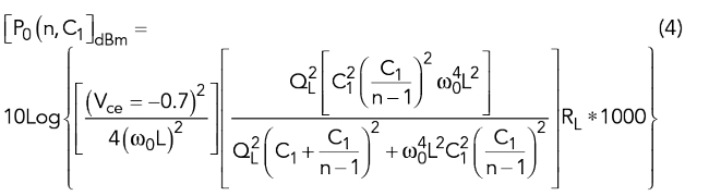
Where 0.7 V is the high current saturation voltage and Vce is the collector emitter voltage < Vcc.