
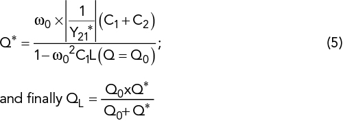
To calculate the loaded Q (QL) consider the unloaded Q (Q0) and the loading effect of the transistor. There we consider the influence of the large signal condition Y21*. The inverse of this is responsible for the loading and reduction of QL.
The transistor noise factor can also be calculated under large signal conditions. Considering Y21*, this noise calculation is based on general noise calculations such as those of Pucel and Rohde.10 An equivalent procedure can be found for FETs as well.
Oscillator Noise Factor
Figure 4 shows the oscillator equivalent circuit configuration for the purpose of analyzing F with respect to the oscillator feedback components (C1 and C2), which are needed to predict F in Leeson’s Equation. The objective is to determine the oscillator circuit parameters that influence F, thereby influencing oscillator phase noise.
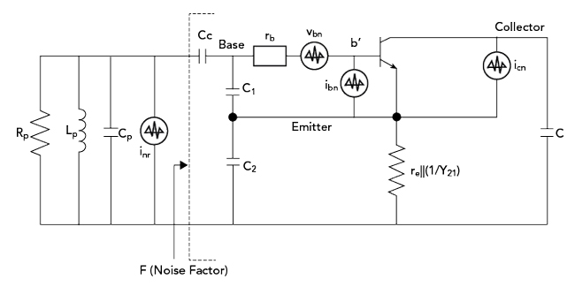
Figure 4 Colpitts oscillator circuit configuration.
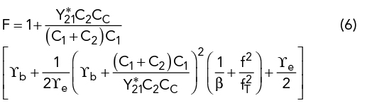
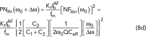
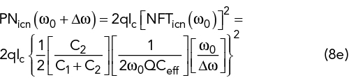
F for the transistor in Figure 4 is:
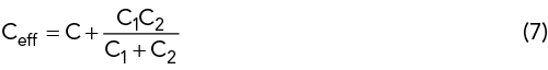
For fixed capacitors C1, C2, the following components contribute to oscillator noise:
- Thermal noise associated with the loss resistance of the resonator
- Thermal noise associated with the base resistance of the transistor
- Shot noise associated with the base bias current
- Shot noise associated with the collector bias current.
An oscillator circuit with the contribution of all four noise sources is shown in Figure 5.
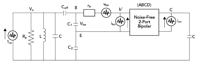
Figure 5 Oscillator calculation using the ABCD matrix.3, p. 132
Using an oscillator circuit with a noisy resonator, the total noise of the oscillator in Figure 5 can be determined.3 Consider the effective capacitance Ceff:
The phase noise contribution (PN) from the oscillator circuit with a 2-port [ABCD] matrix is:
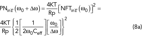
= the phase noise contribution from the resonator tank.
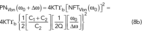
= the phase noise contribution from the base spreading resistance. 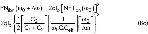
= the phase noise contribution from the base current.
= the phase noise contribution from the flicker noise of the transistor.
= the phase noise contribution from the collector current.
AM-to-PM Conversion
The transition from a basic oscillator to a VCO is achieved by replacing all or a part of the resonator capacitor with a voltage dependent variable capacitor, typically a tuning diode or varactor.2 The RF voltage across the depletion capacitance modulates the operating frequency. FM and PM cannot be distinguished at a constant fm; however, with a change in fm, the FM modulation index will change and the PM modulation index will not.
To calculate the total phase noise, an equivalent noise resistance Req of the tuning diode is defined. When inserted in Nyquist’s equation it results in a frequency offset dependent noise voltage Vn across the tuning diode:

where kT = 4.2 × 10×-21 at 300 K, and Δf is the offset from the carrier.
This noise voltage generated from the tuning diode is now multiplied with the VCO gain Ko, resulting in an rms frequency deviation Δfrms. This can be translated into an equivalent peak phase deviation θd:
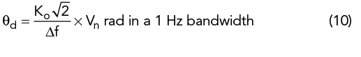
This is converted into the single sideband (SSB) signal-to-noise ratio expressed in dB

Comparing the SSB noise of the oscillator with a fixed capacitor and an identical capacitance value of the tuning diode determines the equivalent noise resistor Req. The lower the resistor the better the quality of the diode. All relevant information is provided by Rohde and Rudolph.9
DIODE FABRICATION AND SINGLE DEVICE PERFORMANCE
A Si tuning diode consists of a p-n junction. Contacting an n-doped and a p-doped region, the mobile charge carriers (electrons and holes) are pulled away from the junction and a depletion zone is created that acts as a capacitor. By applying a reverse bias voltage (V) the depletion zone width xD increases. For the n-type region it is given by:
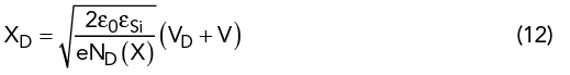
ε0εSi is the dielectric constant of Si, e is the elementary charge and ND(x) is the donor concentration. The diffusion voltage VD is given by:
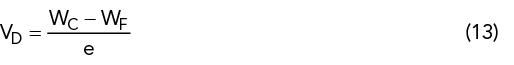
where Wc is the energy of the conduction band edge and WF is the Fermi energy.
For the p-type region, the donor concentration is replaced by the acceptor concentration.
The voltage dependent capacity C(V) can be written as:
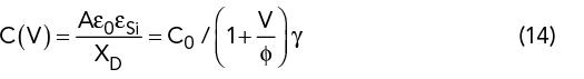
where γ = 0.5 characterizes the theoretical value for an abrupt junction diode with constant doping concentration in the depletion zone.
For a VCO, several more parameters must be considered, such as frequency range, linearity, series resistance and noise level. So-called hyperabrupt tuning diodes11 are widely used for VCOs and this article presents results regarding these requirements. Using epitaxy, ion implantation and careful thermal management, high-quality hyperabrupt diodes are realized with extremely low noise levels.
Highly doped n-type 200 mm Si wafers with (100) orientation are used to achieve low series resistance. In a first step, an n-type epitaxial layer with a thickness of several micrometers and a doping concentration in the range of 1×10¹⁵ to 1×1016 cm-3 is grown. The p+-region is fabricated by ion implantation.
A SIMS profile of the total stack after annealing is shown in Figure 6. In principle it is possible to create even sharper doping transitions,12 however, these techniques (e.g. molecular beam epitaxy) are not suited for mass production. To avoid lateral spreading of the electric field, a guard ring structure is integrated. Diodes with an active area of A = 0.118 mm2 as well as A = 0.037 mm2 are fabricated on the same wafer. For the front-side metallization a Ti/TiN barrier is sputtered followed by Al/1%Si. For the backside a gold-based metallization is chosen to enable soldering in the package.
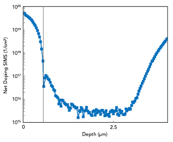
Figure 6 SIMS profile of the hyperabrupt tuning diode.
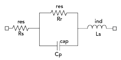
Figure 7 Diode equivalent circuit.
The noise of the hyperabrupt diodes—and therefore the resonator noise—depends on the quality factor Im(Z)/Re(Z). The higher the quality factor of the resonator, the lower the oscillator noise. Considering the equivalent circuit of the diode (see Figure 7), one must consider two parameters:
1) The crystalline quality of the Si in the depletion zone should be as high as possible to avoid any point defects such as vacancies or interstitials, which act as scattering centers and increase the noise level.13 As a consequence, the resistance Rr for reverse bias must be as high as possible. This can be achieved by careful annealing steps.