
2) The real part of the impedance, which mainly consists of the contact series resistances and the wiring of the package, must be minimized. For this purpose, the wafers are thinned to 120 μm. The resulting series resistance Rs of the bare die, measured at 5 GHz and 2 V reverse bias voltage, amounts to 0.8 Ω for the larger diode and 1.3 Ω for the smaller diode.
Wafer Level Measurements
The breakdown voltage for both types of diodes is 31 V. For the larger diodes, wafer level measurements of capacitance (measured at 500 MHz) as a function of reverse bias voltage is shown in Figure 8. A capacitance C1 = 19 pF is measured at a reverse bias of 1 V and C25 = 2 pF at 25 V. The resulting capacitance ratio C1/C25 is 9.5.
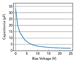
Figure 8 Capacitance tuning range vs. reverse bias on the A = 0.118 mm2 diode measured at 500 MHz.
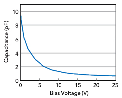
Figure 9 Capacitance tuning range vs. reverse bias on the A = 0.037 mm2 diode measured at 500 MHz.
For the smaller diodes, capacitance versus voltage behavior is shown in Figure 9. A capacitance C1 = 6.2 pF is measured at a reverse bias of 1 V and C25 = 0.75 pF at 25 V. The resulting capacitance ratio C1/C25 is 8.3.
In contrast to the above derived simple depletion approximation, the γ-value of hyperabrupt tuning diodes is no longer constant with reverse bias, however, this value is important for the design of oscillators. Therefore, wafer level measurements are made for the two types of diodes (see Figures 10 and 11).
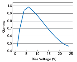
Figure 10 γ vs. bias voltage for the A = 0.118 mm2 diode measured at 500 MHz.
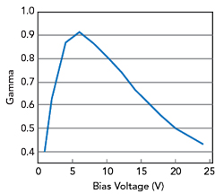
Figure 11 γ vs. bias voltage for the A = 0.037 mm2 diode measured at 500 MHz.
Packaging
After wafer level measurements the wafers are diced and packaged in a QFN type housing with SC79 soldering pads. The front-side contact, which acts as anode, is gold wire bonded, whereas the backside contact, which acts as cathode, is connected to the ground plate. The lead frame is copper.
SIMULATION AND MEASUREMENT OF PHASE NOISE IN A TEST OSCILLATOR
Noise performance of diodes can only be characterized in a test oscillator. It should be noted that different results are obtained for different oscillator designs. The quality of the diodes is demonstrated with the Infineon transistor BFP 620 in an oscillator at 1.3 GHz (see Figure 12).
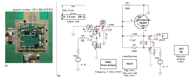
Figure 12 1.3 GHz test oscillator with tuning diodes (a) and schematic (b).
Instead of the tuning diodes, we start with a fixed capacitor of 15.3 pF in parallel with the 0.7 pF capacitor to ground (see Figure 12b), for a frequency of about 1.3 GHz. This is the ideal case and acts as a reference.
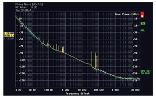
Figure 13 Measured phase noise of the oscillator with a fixed capacitor.
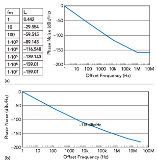
Figure 14 Oscillator phase noise without a tuning diode calculated using Leeson’s equation (a) and simulated using the Serenade HB microwave simulator (b).
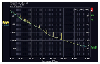
Figure 15 Measured phase noise of the oscillator with tuning diodes.
The measured phase noise of this circuit as a function of frequency offset from the center frequency is shown in Figure 13. At an offset of 10 kHz it is about -115 dBc/Hz. An offset frequency of 10 KHz is used as this is the closest to the carrier selected in a PLL to compensate microphonic effect and outside the PLL loop frequency where the inherent phase noise dominates. The prediction from the presented model as well as the SPICE data-based simulation (see Figure 14) agrees well with the measurement.
Next, the capacitor is replaced by a tuning diode to realize a VCO. According to Figure 8, a reverse bias of about 2 V is needed to obtain a comparable capacitance of 15 pF. The resulting measured phase noise plot of the oscillator is shown in Figure 15. The phase noise at a 10 kHz offset is about -107 dBc/Hz, only 8 dB above the level with a fixed capacitor, for an oscillator with a 2 to 1 tuning range. To our knowledge, this is the best value achieved to date.
Equations 9 and 10 are used to perform a backward calculation for the equivalent noise resistor.
For L(fm ) =-107.41 dBc/Hz,
assuming a K0 of 120 MHz/V, Δfrms = 0.06 in a 1 Hz bandwidth.
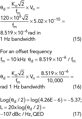
The resulting voltage value Vn = 5.02 × 10⁻¹⁰V√Hz. Finally, the newly developed diodes have a very low equivalent noise resistance of only 15 Ω.
CONCLUSION
The described noise model for VCOs proves that tuning diodes dominate the sideband noise of oscillators. As a figure of merit for the diodes, an equivalent noise resistor is introduced that describes the noise spectrum deviation from an ideal case with a fixed capacitor. The newly developed diodes with the same AC characteristics as commercial diodes demonstrate phase noise levels only 8 dB above the value for a fixed capacitor when measured with the same test oscillator.
References
- E. H. Colpitts, “Oscillation Generator,” U.S. Patent No. 1 624 537, February 1918.
- U. L. Rohde and A. M. Apte, “Everything You Always Wanted to Know About Colpitts Oscillators,” IEEE Microwave Magazine, Vol. 17, No. 8, August 2016, pp. 59–76.
- U. L. Rohde, A. K. Poddar and G. Böck, The Design of Modern Microwave Oscillators for Wireless Applications, John Wiley & Sons, Hoboken, NJ, 2005.
- K. Kurokawa, “Some Basic Characteristics of Broadband Negative Resistance Oscillator Circuits,” The Bell System Technical Journal, Vol. 48, No. 6, July-August 1969, pp. 1937–1955.
- U. Rohde, A. Poddar and A. Apte, “How Low Can They Go, Oscillator Phase Noise Model, Theoretical, Experimental Validation, and Phase Noise Measurements,” IEEE Microwave Magazine, Vol. 14, No. 6, September/October 2013, pp. 50–72.
- E. J. Baghdady, R. N. Lincoln and B. D. Nelin, “Short-term Frequency Stability: Characterization, Theory, and Measurement,” Proceedings of the IEEE, Vol. 53, No. 7, July 1965, pp. 704–722.
- D. B. Leeson, “A Simple Model of Feedback Oscillator Noise Spectrum,” Proceedings of the IEEE, Vol. 54, No. 2 February 1966, pp. 329–330.
- G. Vendelin, A. M. Pavio, U. L. Rohde and M. Rudolph, Microwave Circuit Design Using Linear and Nonlinear Techniques, John Wiley & Sons, Hoboken, NJ, 2021.
- U. L. Rohde and M. Rudolph, RF / Microwave Circuit Design for Wireless Applications, Second Edition, John Wiley & Sons, Hoboken, NJ, 2013.
- R. A. Pucel and U. L. Rohde, “An Exact Expression for the Noise Resistance R/sub n/ for the Hawkins Bipolar Noise Model,” IEEE Microwave and Guided Wave Letters, Vol. 3, No. 2, February 1993, pp. 35–37.
- R. Kumar and A. Bhattacharyya, “Variability Study and Design Considerations of P-N Junction Hyperabrupt Varactor Diodes,” IEEE Transactions on Electron Devices, Vol. 24, No. 10, October 1977, pp. 1270–1272.
- I. Eisele, “Delta-Doping Profiles in Silicon,” Applied Surface Science, Vol. 36, No. 1–4, 1989, pp. 39–51.
- J. Störmer, P. Willutzki, D.T. Britton, G. Kögel, W. Triftshäuser, W. Kiunke, F. Wittmann and I. Eisele, “A Slow Positron Lifetime Study of the Annealing Behavior of an Amorphous Silicon Layer Grown by MBE,” Applied Physics, Vol. 61, July 1995.