
Several years ago, development on mmWave AESA started with cooperative research with AFRL. Cobham Advanced Electronic Solutions (CAES) has enjoyed many years of successful technology development transitions into multiple DoD programs for MMICs and phased array programs. Going forward, constant independent research and development (IRaD) funding has been applied toward developing this critical new technology. When CAES acquired Aeroflex Corporation in 2014, the CAES technology portfolio expanded to include many new, reliable, advanced packaging and assembly options, including flip-chip, bumped die and packages. Among those technologies, the incumbent semiconductor business with broad and deep experience for the high reliability space and medical semiconductor industry - including LEAN Rel™- is enabling small integrated AESA arrays for DoD applications. With ongoing development, these advanced process options are constantly upgrading.
A tailored approach to building AESA systems utilizing new technology offers cost, size, reliability and performance advantages. AESA markets under consideration include - but are not limited to - air surveillance including airborne early warning radar, intercept or acquisition control, ballistic missile warning and acquisition, surveillance, mapping and missile tracking and guidance. Frequencies under consideration include Ka-Band and W-Band. These mmWave steerable systems track target range, position and velocity vectors. Target detections must be resolvable from each other even when targets are substantially contrasting in reflection cross-sections at variable range. Key performance criteria include simplifying the array control and system interfaces with higher levels of integration.
TECHNOLOGY APPLICATION
mmWave phased array dimensions with typical λ/2 element spacings are very small (approximately 5 mm at 30 GHz to 1.9 mm at 80 GHz). Therefore, placing transmit and receive elements at the aperture is feasible and is nearly ideal for T/R electronics at lower mmWave frequencies using quad-channel MMICs and Silicon ICs. Communication arrays are well suited for these form factors with transmit power at less than 0.2 W/element where silicon technologies match the application. Phased array with transmit powers greater than 0.75 W/element require more sophistication in TR electronics and often require active cooling within the array. Fortunately, exotic cooling substrate materials and techniques are not required for power densities lower than 10 W/element. The total transmit power for small arrays is primarily limited by available prime power and the dissipated power in the form of heat generated from each element’s T/R amplifiers RF conversion efficiency. At mmWave frequencies, the factor limiting operation is typically heat dissipation. Power added efficiency at mmWave - established by semiconductor technology and circuit implementation - should be 5 percent or higher for a multi-stage MMIC amplifier.
There are many mechanical concerns in constructing mmWave arrays. Key concerns include - but are not limited to - supply voltage current density on voltage supply lines, location of the RF, DC and control lines. In the case of higher transmit power, active cooling may be required for long term operation.
Higher operating drain voltages of GaN MMICs help lower current density in connectors and distribution networks. GaN on SiC MMICs offer the thermal advantages of SiC to spread the heat from the transistor and passive heat sources within the MMIC. DC and RF connectors and interconnects present problems as they are a notable source of RF losses and increased product cost.
Likewise, space-consuming interconnects have a direct impact on array scalability and overall cost. It is challenging to build scalable mmWave phased arrays with λ/2 spacing while using the smallest available RF connectors, in addition to being cost-prohibitive. While there have been many advances in mmWave and RF connectors over the past few years, the best way to leverage their impact is through higher levels of integration within the array aperture. Further, the implementation of these arrays into application platforms demands as much simplification as possible to optimize size and performance, and for electrical and thermal interconnects. When building arrays within the Ka-Band frequency range, it has become increasingly obvious that higher levels of integration with customized SoC and automated assembly processes drive performance and affordability toward planar phased array architectures.
KA-BAND PHASED ARRAYS
Since 2016, core building blocks built from custom ICs and packaging technology have been specifically created for Ka-Band AESA hardware. Key pieces of the development include, 1) multi-channel Silicon-Germanium (SiGe) beam-former ICs, 2) multi-channel GaN T/R MMIC with PA, LNA, switches, et. al., 3) chip-scale flip-chip packaging (K-CSP) for both die on organic substrate, 4) integrated heat sink and 5) I/O RF, DC and control signals. The silicon die utilizes solder bump flip-chip technology, and the GaN MMIC die utilizes Cu pillar flip-chip technology. The K-CSP configuration leverages production flip-chip processes developed and qualified to QML Class-Y. These are automated processes for environmentally extreme rugged use conditions. The MMIC and mmWave SoC combination was designed a few years ago with specific features needed for phase array operations.
Currently, the GaN T/R MMIC is a multi-channel mmWave RFIC with approximately 15 percent bandwidth and electrical channel-to-channel symmetry. The T/R MMIC has ≥ 1 W/channel transmit output power and ≤ 5.5 dB receive noise figure as integrated with low insertion loss T/R switches. PA efficiency, LNA noise figure and T/R switch power handling and loss were optimized to near performance limits offered by short gate length GaN technology. The SiGe SoC was set up for an analog beamforming to work specifically with the GaN T/R MMIC in a 3D stack. The SiGe SoC has 30 dB amplitude control, and near six-bit phase control. The I/Q performance plane is corrected with built-in coefficients for small and simple calibration stored within on-chip register space. Calibration tables are very small and allow a single 64-bit serial beam-steering command to repoint the entire array with potentially many hundreds or thousands of elements.
Figure 3 pictures the SiGe/GaN test boards used to characterize the channel characteristics, RF and thermal performance and is the basis of the ongoing 8 x 8 phased array modules optimized for organic substrates. With nearly six bits of phase resolution channel performance, the test demonstrated RMS error of 2.4 degrees mid-band phase error and 0.36 dB of mid-band gain error.

Figure 3 K-CSP test board (basis for 8 x 8 array) (a) and SiGe/GaN beam-former I/Q performance, and RMS phase and amplitude error (b).
Figure 4 illustrates a 64-element sub-array and vertically integrated assembly. Extensive reliability analysis (including solder stress and mechanical stress predictions) and environmental test verification offer a path to reliable automated assembly processes for IC integration. These small integrated arrays (38.1 x 38.1 x 20.3 mm) are assembled to withstand austere environments with reliable operation both mechanically and thermally. The use of commonly available organic substrates provides the opportunity to tailor array pattern variation with custom printed circuit board shapes (i.e. round, rectangular, octagonal, etc.). The GaN MMIC has fractional-power modes and may be scaled up in output transmit power to 8 W/element or more for array architectures with a limited number of elements.
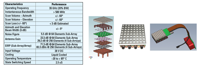
Figure 4 64-element planar Ka-Band test sub-array and performance goals.
The array has a 120-degree field of view with 3 dB beam width of ± 5 degrees and less than 3 dB of scan loss at ± 60 degrees. The effective isotropic radiating power for a 256-element array is approximately 83.3 dBm (≥200 kW) with beam state switching speed of less than 2.5 µs. The radiating elements are circularly polarized, and the current demonstration array is half-duplex. Dual polarization configurations are also under development. The arrays are liquid cooled - with PAO or other suitable cooling liquids - to maintain a uniform temperature and low thermal gradients across the array. Integration of the Ka-Band AESA architecture is scalable into large arrays, or scalable down into arrays with fewer elements as shown in Figure 5.
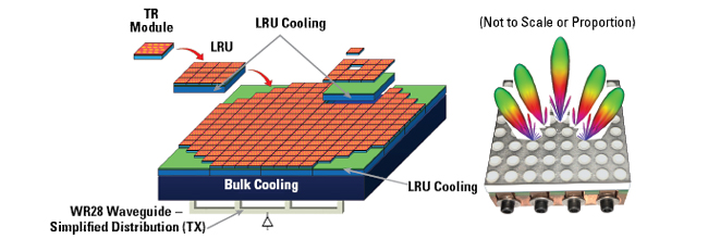
Figure 5 AESA topology scalable from a few elements to 1,000s of elements with LRU building blocks.
Fully scalable arrays require all signals to be routed through the backside of the array (including thermal) and require a blind-mate interconnect solution for both electrical (RF, control and DC) and mechanical (fluid). Each sub-array has a single RF port to be used with a sum and difference mono-pulse comparator for direction finding and tracking. This technology is manufacturable and reliable, with field-replaceable upgrades and improvements. It is also adaptable to changing requirements and technology upgrades, including polarization diversity and other advancing technologies. The applied technologies are quickly advancing manufacturing readiness levels toward production capability.
mmWAVE AESA TECHNOLOGY EVOLUTION- APERTURE TO DATA
Performance advancements in recent years in small geometry Si CMOS technology (including RF CMOS), have allowed higher levels of integration to become a reality. Work extending the multi-channel planar approach of the Ka-Band array to include other key pieces of the radar is underway with architecture studies and demonstrations. This new integration will make ultra-small advanced capability arrays with digital conversion a reality in the coming months and can be shown using mmWave radar demonstrations.
IRaD is currently underway to evolve the up/down converters, transmit signal synthesis (DAC) and receive digitization (ADC) at rates exceeding 1 GS/s and to include radar detection and digital-signal-processed datasets directly in the aperture electronics. This architecture enables multi-beam software-defined digital beamforming (or mixing of digital and analog beamforming). This capability enables digitally modulated radar sensor operation utilizing beamforming and code division multiplexed MIMO radar capabilities. The MIMO feature offers extended virtual receive channels, improved angular resolution and interference immunity associated with digitally coded channels. These extended capabilities also offer improved range resolution, better signal to noise ratio at similar frame rates and faster updates with short system cycles. The system can also switch between phase array modes and massive MIMO processing mode or a combination thereof. Advance digital processing ICs utilizing these capabilities result in 4D detection datasets with spatial position and velocity for many targets. This is the new world of aperture to data.
This architecture offers other advantages. The integration of the RF converter, ADC/DAC and radar data processor into the aperture electronics will drastically simplify interconnect solutions. Traditionally, the direct digital conversion and processing functions have been power-hungry; now these capabilities may be included more efficiently, with less prime power and lower heat generation. mmWave RF connections (coax or wave guide) are no longer needed to route signals throughout the application platform. Interconnect simplicity is achieved by way of high-speed data uplinks (10/100 Gbit/s) through Ethernet or proprietary vehicles - along with simple DC supply line distribution - making radar and sensor aperture deployment easier and faster. Further, widely used production processes for fully automated assembly processes are utilized to minimize human touches, improve reliability, eliminate tuning and ruggedize the platform for austere environments and challenging operating conditions. Improved system performance (associated with RF signal loss), simpler interconnects, faster integration, smaller size and weight and lower cost offer overall system value.
SUMMARY
The extended capabilities and value proposition associated with integrated and multi-mode mmWave array technology include:
- Advanced packaged 3D electrical and thermal integration at the aperture
- SiGe beam-formers and advanced custom CMOS ICs for advanced functionality
- Higher transmit power and rugged assemblies for integrated multi-channel GaN T/R MMICs
- Multi-channel digitally coded phased array, MIMO sensor capabilities
- Mono-pulse direction finding
- Advanced angular resolution
- Improved Doppler
- Multiplicity of scans in compressed scanned times
- Fast uplink
- Simpler integration and deployment
- Smaller packages (size and weight)
- No tuning automated assembly
- Lower cost
- Scaled solutions (from a few elements to 1,000s of elements)
- Integrated “aperture to data” architecture
It is a great time to be involved in today’s battlefield, which is simplified by the value proposition of advanced technology solutions for broad deployment to the warfighter.