Phased array radar systems use many transmit (Tx) and receive (Rx) channels to create steerable beams. Historically, these platforms were built using separate Tx and Rx ICs, including separate digital-to-analog converters (DAC) in the Tx chain and analog-to-digital converters (ADC) in the Rx chain. The use of discrete ICs led to large footprint, high-power consumption, high cost systems with long time to market, due partially to the manufacturing and calibration complexities. A newer approach uses integrated transceivers that combine the discrete functions into a single IC, enabling smaller, lower power consumption and lower cost phased array radar platforms with faster time to market. This article will discuss the benefits enabled by integration.
Integrated transceivers combine multiple functions onto a single IC, simplifying system design and streamlining a customer’s time to market. The latest transceivers integrate DACs, ADCs, local oscillator (LO) synthesizers, microprocessors, mixers and more functions into a single monolithic chip, such as Analog Devices’ 12 mm x 12 mm ADRV9009 (see Figure 1). This product combines two Rx channels and two Tx channels with digital signal processing (DSP) and achieves 200 MHz Rx bandwidth and a tunable Tx bandwidth of 450 MHz. An application program interface (API) is provided to program and control the transceiver from the customer’s platform. Gain and attenuation can be controlled using the on-chip front-end networks, and built-in initialization and tracking calibration routines provide the performance required for many communications and military applications.

Figure 1 The ADRV9009 is an example of an integrated transceiver that combines RF and digital functions on a single IC.

Figure 2 Phase can be aligned to a reference source with the RFPLL phase sync enabled (a) vs. disabled (b).

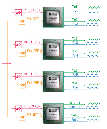
Figure 3 The number of system channels can be increased using additional transceivers.
The integrated transceiver creates all the clock signals needed for Tx and Rx, injecting a single reference clock signal known as REF_CLK. On-chip phase-locked loops synthesize all the required clocks for DAC and ADC sampling, LO generation and the microprocessor. If the internal LO phase noise does not meet system requirements, the user can inject an external LO with lower phase noise. Data from the transceiver is offloaded via a standard JESD204b multigigabit serial data interface, enabling large amounts of simultaneous data for Tx and Rx. If deterministic latency and data synchronization are needed, the user can use the built-in multichip synchronization (MCS) feature and issue a SYS_REF signal to act as a master timing reference for an initial lane alignment sequence (ILAS).1 The LO phase of a Tx or Rx channel can be deterministic with respect to a master reference phase using the built-in RFPLL phase sync feature. By using both the MCS and the RFPLL phase sync features, phase alignment can be replicated when initializing the transceiver, frequency tuning or toggling the radio on and off via the control software (see Figure 2).
MULTIPLE INTEGRATED TRANSCEIVERS
If more than two Rx and two Tx are required for a system, the user can use multiple transceivers and benefit from the small size achieved with monolithic integration (see Figure 3). Multiple transceivers can be synchronized using concurrent SYS_REF pulses to simultaneously trigger internal dividers for all the ICs. These SYS_REF pulses can be issued by either clock chips or baseband processors with programmable delays, to account for any length mismatches between the routes to the various ICs. Both the data paths and multiple LOs across multiple ICs are capable of being deterministic.
