

Overview
Engineers can use a variety of methods to analyze the behavior of a voltage regulator module (VRM) using frequency and time-domain techniques, as we have seen starting from Part 6 in this series of articles. Part 10 showed how the load transient response to a step change or impulse in the time domain can reveal the frequency-domain characteristics of the output impedance (ZOUT) of a VRM.
Another approach to using the load transient responses to step changes is to use the technique embodied by the Stability Evaluation for Power Integrity Analysis (SEPIA[i]) software, developed by Steve Sandler of Picotest. This analysis can be performed using simulations or bench-test waveform data recorded from physical devices.
The SEPIA method takes advantage of the assumption that any circuit that acts as a filter will demonstrate similar ringing profiles in response to a step load. If they share the same quality factor (Q) they will exhibit the same ringing profile as long as the underlying system demonstrates quadratic behavior. Take the plot in Figure 1 as an example, which was generated from a simulation described later in this article. With a Q of 5.52, it responds with 20 readily detectable ringing peaks. Variations in system setups will lead to different ringing frequency, amplitude and DC bias. But all of the systems with a Q of 5.52 will share the same numbers of peaks and with the same decay rate.

Figure 1. Ringing Peaks from a System of Quality Factor Q = 5.52
Thanks to this relationship, we can obtain a value of Q for an unknown system based on the ringing waveform by applying a step load. As well as using this relationship to provide the Q for an unknown system, the SEPIA software can use textbook formulas to estimate the parameters of components in the target circuit.
To maintain high accuracy, the step load needs a rise or fall time that is as fast as possible and minimally capacitive, where faster than 35% of maximum measurement bandwidth or at least five times faster than the DUT control loop bandwidth. Once the loop information is extracted, the SEPIA software performs a parameter fitting procedure to build quadratic circuit models.
To confirm the accuracy of the SEPIA-based technique, we can perform an experiment using a pair of simulations. These two simulations model VRMs that have an equivalent structure that can be modeled quadratically, but which have different placements for the dampening resistors. By feeding the result from the first SEPIA analysis into a second SEPIA process, as shown in Figure 2, we can confirm that the results are identical and, therefore, confirm the technique works as expected.
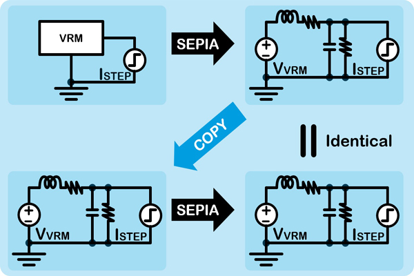
Figure 2. Confirmation: SEPIA Extracting Correct Parameters in a Chain
Armed with all the methods for assessing ZOUT described from Part 6 in this series to the SEPIA method, we can perform a detailed analysis of a step-down (buck) DC/DC regulator with unknown properties as our VRM target in the second half of this post.
Simulations
The simulations in these experiments were all run using QSPICE™, with the SEPIA procedure captured as a QSPICE user-defined block written in C++. Labelled as SEPIA@QSPICE block, it is included in the simulation decks Qorvo has made available in its repository on GitHub. Together with PyQSPICE module written in Python, this module handles all the data arrangement, calculation, plotting, and recording of the operations performed using the Jupyter Lab platform.
1st Simulation, SEPIA Reproducing its Input: Model-0
Model-0, Schematic
Because this is a simple RLC resonant circuit, we can analyze its performance in a reasonably straightforward way using an AC simulation. However, it is not always easy to run an AC simulation of VRMs. This is where methods such as SEPIA demonstrate their value.

Figure 3. SEPIA@QSPICE Model-0 Schematic
In this model, the key contributions to the damping resistance come from the inductor’s DC resistance (DCR) and the capacitor’s equivalent series resistance (ESR). The equation below can be used to compute the Q of this circuit.
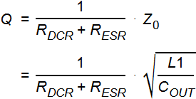 Eq.11-1
Model-0, SEPIA Report / Log
When the simulation runs, the gray-box monitor of our SEPIA@QSPICE block detects each of the ringing peaks and minima on-the-fly. This output is shown as the orange curve in Figure 4, providing timing and amplitude data for analyzing the decay profile using the SEPIA routine.

Figure 4. SEPIA@QSPICE Block On-The-Fly Peak Detection
At the end of a simulation, the SEPIA block outputs the following information:
- Report / Log File
- Transient Simulation Deck
- AC Simulation Deck
The log file is text-based and shows how the SEPIA block dealt with the results of the simulation. Looking at the text highlighted in red, we can see the component parameters extracted by the SEPIA module. Comparing them with the values on the schematic, we can see they were extracted successfully.
======== SEPIA Result Begin ========SEPIA: Q= 5.57, Icoil/2=2.22e-15, f=70.89(kHz), T=14.11(us), PM=10.26(deg),SEPIA: Z=2.24e-02, L=4.98e-08, C=9.96e-05,SEPIA: (sL+Rcoil) // ((1/sC)+Rcap) Modeling Rcoil+Rcap=4.02e-03, Rcoil=2.00e-03, Rcap=2.02e-03,SEPIA: (sL) // (1/sC) // Rdump Modeling Rdump=1.24e-01, Rcoil=2.00e-03,SEPIA: preAve=5.00e+00, postAve=5.00e+00======== SEPIA Result End ========The simulation deck outputs are QSPICE input files that are ready to run. The circuit models they contain are identical but use different QSPICE simulation directives: ".TRAN" or ".AC". We can see how they compare. Readers who want to see the details can refer to the session file.
Model-0,Transient Response
When we observe the QSPICE simulation of the SEPIA module’s output compared with the simulation of the original schematic, we confirm that we have identical curves in the time-domain with no apparent differences.

Figure 5. SEPIA@QSPICE Model-0 Transient Response Comparison of the INPUT and OUTPUT
Model-0, Output Impedance
Similarly, looking at the output impedance in the frequency domain, we can see that the SEPIA module outputs a curve that is identical to that of the original model.

Figure 6. SEPIA@QSPICE Model-0 Output Impedance Comparison of the INPUT and OUTPUT
2nd Simulation, SEPIA Reproducing its Input: Model-1
Model-1, Schematic
Figure 1 is generated from this Model-1.

Figure 7. SEPIA@QSPICE Model-1 Schematic
In this model, we distribute the damping resistance components provided by the inductor DCR and load resistance R1. The relationship to Q in this circuit is captured by the equation below.
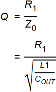 Eq.11-2
Model-1, SEPIA Report / Log
Using the log output from the simulation of Model-1, we can see that the SEPIA module successfully extracted the component parameters (highlighted in red) by comparing them with those on the schematic.
======== SEPIA Result Begin ========SEPIA: Q= 5.52, Icoil/2=2.66e-15, f=70.89(kHz), T=14.11(us), PM=10.35(deg),SEPIA: Z=2.25e-02, L=5.02e-08, C=9.88e-05,SEPIA: (sL+Rcoil) // ((1/sC)+Rcap) Modeling Rcoil+Rcap=4.08e-03, Rcoil=1.01e-06, Rcap=4.08e-03,SEPIA: (sL) // (1/sC) // Rdump Modeling Rdump=1.24e-01, Rcoil=1.01e-06,SEPIA: preAve=5.00e+00, postAve=5.00e+00======== SEPIA Result End ========Model-1, Transient Response
We can observe in the SEPIA output that, when compared with the simulation of the source schematic, we have identical curves in the time-domain with no apparent differences (Figure 8).

Figure 8. SEPIA@QSPICE Model-1 Transient Response Comparison of the INPUT and OUTPUT
Model-1, Output Impedance
The situation is the same for the frequency-domain analysis. Once again, and as anticipated, we can see that the SEPIA model outputs an identical curve to the original model (Figure 9).
Figure 9. SEPIA@QSPICE Model-1 Output Impedance Comparison of the INPUT and OUTPUT
Analyzing a VRM of Unknown Loop, Simulation #3
When evaluating a VRM on the test bench, it is rare that we can perform a simple AC simulation to determine the closed-loop performance of the module. It is often a black box. Engineers may find that while creating independent models for analysis using transient and AC simulation modes, a lot of time is spent trying to prove that they both deliver accurate representations of the target circuit.
However, when dealing with a DUT that has unknown loop performance, you can guarantee that it is always possible to measure the output voltage port and use that data to determine ZOUT, stability, and transient response. Starting from Part 6 of this series, we introduced various techniques for using a VRM’s ZOUT in both time-domain and frequency-domain to deliver accurate results.
To summarize this work on ZOUT, we can analyze a switched-mode step-down (buck) DC/DC regulator.
Analyzing Strategy
The procedure involves seven steps detailed below, which are available in the session file for Simulation #3 on Qorvo’s Github repository.
1. Simulation #3-1
Perform a transient simulation of the circuit schematic of the DUT that includes the SEPIA@QSPICE block to deliver the SEPIA results.
We then run the rest of the operations to compare their results with the SEPIA analysis.
2. Simulation #3-2
Perform a transient simulation "transient" model generated by the SEPIA@QSPICE module.
3. Simulation #3-3
Perform an AC simulation on the "AC" model created by the SEPIA@QSPICE module.
4. Simulation #3-4
Perform an AC simulation on the original schematic but ensure the VRM stays off to provide ZOUT(VRM=OFF).
Here, we can run AC simulation because the VRM stays in its off state.
5. ZOUT Calculation
Based on the procedure described in Part 10, and using the model developed for Simulation #3-1, we extract ZOUT(VRM=ON) by taking the Laplace transform of the derived step load response. Then, using the procedure from Part 8, we can reconstruct the loop-transfer function using the ZOUT(VRM=ON) and ZOUT(VRM=OFF) values as inputs.
6. Import Fully Validated Transfer Function Prepared Offline
Though we don’t review the details here, we can import a dataset generated from a fully validated AC simulation of the DUT’s VRM design and use that as a reference.
7. Validation / Comparison
Armed with these different results, we can compare the DUT’s loop-transfer function. To summarize, those results consist of:
the SEPIA result from simulation #3-1; a reconstructed loop-transfer function created using the techniques in step 5;
and the imported data described in step 6.
DUT-Buck Schematic
Figure 10 shows the schematic of our DUT: a buck regulator, producing a 3.3 V output from a 5 V input. It has several important elements. It employs constant-ON-time (COT) control with coil-current feedback for loop compensation. The output capacitor is assumed to be a device with a very low ESR that is typical of a multi-layer ceramic capacitor (MLCC).

Figure 10. Unknown Loop Step-Down VRM Schematic
Step-1: Simulation #3-1
======== SEPIA Result Begin ========SEPIA: Q= 1.54, Icoil/2=1.54e-03, f=17.75(kHz), T=56.34(us), PM=35.73(deg),SEPIA: Z=4.26e-02, L=3.45e-07, C=1.91e-04,SEPIA: (sL+Rcoil) // ((1/sC)+Rcap) Modeling Rcoil+Rcap=2.76e-02, Rcoil=1.43e-05, Rcap=2.76e-02,SEPIA: (sL) // (1/sC) // Rdump Modeling Rdump=6.57e-02, Rcoil=1.43e-05,SEPIA: preAve=3.30e+00, postAve=3.30e+00======== SEPIA Result End ========Because this is a switch-mode power supply, the output voltage waveform will demonstrate switching ripple that makes it harder to focus on the core ringing profile. To deal with this issue, we filter out the raw output voltage waveform using a moving-average filter. Figure 11 shows the original and filtered time-domain response of simulation #3-1.

Figure 11. Step Load Transient Response of Original Step-Down VRM, Moving Average Filtered
Step-2: Simulation #3-2
Using the transient model of the buck regulator generated by the SEPIA module in Step #3-1, we run a simulation and compare it with the original simulation result, as shown in Figure 12. Note that the simulation trace from Step #3-1 starts with an output voltage of zero which invokes the regulator’s slow-start function. The SEPIA-extracted model starts directly from 3.3 V DC.
As we can observe, the SEPIA program extracted the loop parameters and modeled this unknown VRM precisely into a simple RLC circuit with only a small difference in the absolute DC bias point.

Figure 12. Step Load Transient Response Comparison Original Step-Down VRM and SEPIA Extracted Model
Step-3: Simulation #3-3
Similarly, we have the AC model created by the SEPIA module. The simulation of that deck results in the orange curve in Figure 13.
Step-4: Simulation #3-4
While the VRM remains in its OFF state, we can simulate the original buck regulator schematic to evaluate the output impedance in that OFF state. This results in the green dotted-line curve in Figure 13. Note that this step is equivalent to simulating the output-capacitor block on its own. It should also be noted that when analyzing the behavior of a physical evaluation board, we should take into account the DC-bias effects exhibited by MLCCs if they are used.
Step-5.1: Zout Calculation
Using the technique described in Part 10, we reconstruct from Simulation #3-1 the output impedance of VRM in its ON state. Shown as the blue curve in Figure 13, this also includes the plots generated in Steps 3 and 4. We can see the method from Part 10 yields a very accurate reconstruction of the output-impedance curve.

Figure 13. Output Impedance Comparison Original Step-Down VRM and SEPIA Extracted Model
Step-5.2: Loop Transfer Function Calculation
Using the plots created for Figure 13, we reconstruct the loop-transfer function of this VRM[ii] using the technique from Part 8, from the ZOUT(VRM=ON) and ZOUT(VRM=OFF). This creates the blue curve shown in Figure 14.
Step-6: Import Offline Data
Because we are reusing a VRM model from past projects, we already have a fully validated transfer function for it. This data is shown as the orange curve in Figure 14.
Step-7: Comparison
Figure 14 therefore provides a combined result built using Steps 5.2 and 6. Also, from Step 1, using Simulation #3-1, we can plot the ZOUT frequency peak obtained using the SEPIA technique as the green dotted-line cross mark. We can see all three results align well with each other, especially around the unity gain frequency point of 17.8 kHz, which is the area of interest.

Figure 14. Loop Transfer Function Comparison Original Step-Down VRM and SEPIA Extracted Model
Conclusion
As we have seen, the SEPIA technique provides the ability to accurately obtain the loop information for a VRM in a direct and easy manner. It can also create equivalent models using just the step load-transient response using either simulated or measured data. Through a review of techniques presented earlier in this series, we also confirmed that the output impedance characteristics of an unknown system, using both time-domain step-response measurements and frequency-domain ZOUT curve data, provide sufficient information of the system loop transfer function. In addition, we have seen how we reconstruct the loop-transfer function from ZOUT(VRM=ON) and ZOUT(VRM=OFF).