
EMC standards are created to verify the reliability of electronic equipment. The standards need not only dictate the test levels and requirements, but must specify test equipment, configuration and requirements. There exist countless possible RF threats, usually in the form of transmitters, most of which are narrow band. Because it is difficult to predict exactly what sources of interference to which a particular device may be exposed, most EMC test standards specify a broad spectrum approach, including the likely frequencies of all perceived threats:
- Commercial IEC: 150 kHz to 6 GHz
- Military: MIL-STD-461: 10 kHz to 18 or 40 GHz
- Avionics: DO-160: 10 kHz to 18 GHz
- Telecom: Bell Core GR-1089: 10 kHz to 10 GHz
- Automotive: 1 MHz to 18 GHz
The standards specify the field intensity to which a product must be subjected, based on real world field measurements, past failures or even potential future threats. Based on the product's application and the level of product quality, a safety margin is often applied to the level of the perceived threat to ensure the test field exceeds that which the product may encounter in use. The required EMC amplifier power is determined based on these specifications and the gain of the antenna or transducer used to generate the specified field as well as the area to be illuminated.
- Commercial IEC: 30 V/m → 1 kW at 80 MHz
- Military: MIL-STD-461: 200 V/m → 10 kW at 10 kHz
- Avionics: DO-160: 7.2 kV/m pulsed → kWs - MWs
- Telecom: Bell Core GR-1089: 8.7 V/m → low 100s of W
- Automotive: 600 V/m pulsed → 1 kW
Additional amplifier constraints may include limits on harmonic power and linearity since amplifiers, operating in a nonlinear region, will typically generate high harmonic power. When designing narrowband amplifiers, it is possible to realize the biasing and matching circuitry to filter this harmonic power; however, this is generally not possible with multi-octave amplifiers. Beyond this, driving an amplifier into compression leads to distortion, which may produce results that do not duplicate in another laboratory, due to unknown or unpredicted spurious or harmonic power.
A final requirement for the RF amplifiers is ruggedness, both physically and electrically. The normal EMC laboratory environment can be demanding. The antennas and transducers required to generate the field can have very severe mismatches, causing high power reflections that may damage amplifiers not designed for this specific application. Many amplifiers designed to handle poorly matched loads and high power reflections may do so by reducing, or "folding back" the amplifier output power, which may prevent the amplifier from delivering the specified power to a poorly matched antenna. This can make it impossible to meet the field requirements specified by the test standard, so it is critical that any amplifier specified for EMC testing be able to deliver full power into any antenna or transducer it may encounter, without folding back or reducing output power in any way.
The Traveling Wave Tube
Historically, the traveling-wave tube (TWT) amplifier, with the capability to deliver very high power with extremely wide frequency at a reasonable cost, has been the answer to the needs of microwave EMC test engineers. However, increasingly stringent restrictions written into many of the EMC test standards, along with a desire to more closely and carefully control the test environment, has helped solid-state EMC amplifiers to absorb an ever larger portion of this market. The TWT amplifier, with significantly higher broadband noise and harmonic power, poor linearity and mismatch tolerance, typically cannot compete with the performance of a class A, solid-state amplifier.
The Solid-State Amplifier
The explosion of wireless communications has changed the dynamics of power transistor technology development. High volume applications have provided capital for development of devices that provide higher performance than ever before. While the majority of these devices have been tailored to the specific needs of various commercial and telecom applications, a few foundries have released general-purpose transistors using each of these new technologies, allowing the design of solid-state amplifiers with power density previously available only from traveling wave tube amplifiers.

Figure 1 Output power density vs. frequency for various FET technologies.
Most significant in power device technology are the development and widespread use of silicon LDMOS and silicon carbide (SiC) for use at RF frequencies (< 3 GHz), and gallium nitride (GaN) high electron mobility transistors (HEMT) operating in the lower microwave domain (1 to 10 GHz). LDMOS has gained popularity at the expense of silicon bipolar transistors and MOSFETS, while GaN HEMTs offer significantly higher power density than gallium arsenide (GaAs) pseudomorphic HEMTs (PHEMT). SiC devices have provided performance enhancements in the traditional crossover frequency range between silicon transistors and GaAs devices. GaAs PHEMTs and indium phosphide (InP) HEMTs continue to dominate at upper microwave (10 to 30 GHz) and millimeter-wave (> 30 GHz) frequencies (see Figure 1).
At RF frequencies, silicon LDMOS devices offer a revolutionary change in packaging. The device structure provides for the source terminal to be the back side of the die, allowing the die to be attached electrically and mechanically to ground (the package flange). Through careful adjustments to materials and processes, it has become possible to utilize a nearly pure copper flange in some instances, providing extreme improvements in thermal performance over traditional devices, which place an insulating ceramic and a less-conductive composite flange between the transistor die and the heat sink. Plastic encapsulated packages are rendered economically feasible by the volume markets associated with LDMOS devices, replacing ceramic packages at very significant cost reductions.
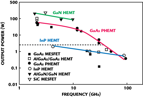
Figure 2 Output power vs. frequency for various power FET technologies.
At lower microwave frequencies, the development of GaN HEMTs has pushed power densities to new limits1 (see Figure 2), reducing the parasitics commonly associated with large GaAs devices and alleviating many problems associated with broadband matching of high-power transistors. This increase in available power does bring increased complexity to power amplifier design, in terms of thermal management and large-signal device characterization, as it is rarely possible to bias GaN HEMTs in a true class A mode of operation without exceeding thermal constraints and damaging or degrading the device. For a generation, microwave engineers have been able to rely on simple small-signal design using S-parameters and linear simulators for designing GaAs-based broadband class A amplifiers. Many are now struggling to understand complex nonlinear behavior and large-signal design techniques required to safely and efficiently extract maximum power from the GaN HEMT, while maintaining the durability and load tolerance they have come to expect from their GaAs counterparts.
An equally important consideration to the actual device technology employed is the packaging of the device. Package material and mechanical considerations define the thermal characteristics of the packaged transistor, as well as the amount and configuration of wire bond inductances and package lead capacitances and inductances that affect the ease or difficulty with which the packaged transistor can be impedance matched for maximum power and gain over a given range of frequencies. These small parasitic inductances and capacitances produce reactances often safely neglected at RF frequencies, generally below 1 GHz, but become very problematic for broadband matching at microwave frequencies.
The thermal constraints imposed by the high drain currents and voltages possible, with many of the newer device technologies, creates problems that are altogether new to most microwave engineers used to working with devices operating at significantly lower power densities. RF engineers working below 1 GHz have worked with these constraints for many years using more powerful devices than those classically available to the microwave engineer, but are also facing new challenges due to increasing power density of SiC and LDMOS. In both cases, the primary challenge is developing methods to dissipate more heat from smaller parts, requiring more research and development in heat sinks and heat spreaders than previously required of RF and microwave amplifier manufacturers.
Key Amplifier Design Considerations
Because the antennas, connected to the amplifier in an EMC test environment, often present high VSWR, special consideration must be given to amplifiers designed for EMC testing applications, such that they can drive full power into loads ranging from a near-short circuit to a near-open circuit. This factor, more than any other, presents serious problems for the engineer, as the bandwidth of the amplifier is usually far too great to consider the use of circulators or other isolating devices. The problem is further aggravated by many of the newer transistor technologies, whose thermal constraints prevent the engineer from biasing the transistors in the mode classically shown to be most favorable to tolerating these conditions.
Every transistor has intrinsic characteristic input and output impedances, governed both by the material form and structure, with which the device is constructed. Extrinsic parasitic conductance and susceptance is added to this, due to the necessary interconnects on the chip and packaging surrounding the chip, adding up to a total input and output impedance that varies with frequency, bias and drive conditions, but which also must be well-matched at all frequencies for a given bias and drive condition. Once an appropriate bias is selected for a device, the primary responsibility of the RF/microwave engineer is to design circuitry that will provide the appropriate impedance matching to the input and output of the transistor, permitting the maximum transfer of power by controlling the voltage and current magnitude and relative phase.
Traditionally, this has been accomplished by measuring the S-parameters of the device, composed of the forward- and reverse-traveling voltage and current waves resulting from small-signal (that is very low power) stimulus at each device terminal, most often base and collector or gate and drain for bipolar and field-effect devices, respectively. Simple mathematical calculations allow one to correlate the magnitude and phase of these waveforms to characteristic impedances for the device at each frequency, operating at a given bias.
The characteristic behavior of most RF/microwave transistors in use over the last several decades has allowed this to work quite well by providing a "strong nonlinear" response that stays very linear from small-signal conditions to a level very close to the maximum power of the device, before sharply transitioning into current saturation. For years, only RF/microwave engineers designing high-efficiency power amplifiers had to give special consideration to nonlinear effects, and even then, design from S-parameters was most often sufficient.

Figure 3 Strong and weak nonlinearity, as related to a FET.
Unfortunately, many of the newer devices discussed herein display a "weak nonlinearity," in which the device gradually transitions from a linear small-signal response into saturation over a wide range of drive conditions (see Figure 3). The strongly nonlinear device (solid line) has well-defined break points with an entirely linear relationship between drain current and gate voltage from Id to Imax, whereas the weakly nonlinear device (dashed line) has poorly-defined break points and a gradual roll-off in Id from bias to Imax. This all but eliminates the possibility of finding ideal matching conditions based on S-parameters alone, confounding many engineers used to working with more traditional device technology. Rather than working directly from S-parameters or using linear circuit simulators, it is necessary to construct complex nonlinear device models and employ long-forgotten methods to find the ideal matching conditions for extracting maximum power or efficiency from this new breed of transistor.
Thermal considerations further complicate the development process, especially for those designing broadband amplifiers around these new device technologies. Thermal resistance and junction temperature constraints rarely allow the engineer to bias the device in a true class A mode of operation. Unfortunately, traditional techniques developed for eliminating the harmonics generated when driving a device under large-signal conditions cannot be employed in multi-octave amplifiers, as the harmonics of the lower frequencies of operation are now "in-band."
It is necessary to carefully study the behavior of the device under a wide range of bias and load conditions in order to find the ideal compromise between thermal and electrical performance, which can be extremely time consuming at best. This requires design techniques, nonlinear device models, and simulators of a complexity with which most RF/microwave engineers are not familiar. The specialized field of nonlinear device modeling, long used by engineers working on high-efficiency power amplifiers, is becoming more relevant as manufacturers of these new devices scramble to provide models of a complexity with which they are often unfamiliar. Some have employed the expertise of companies and university laboratories specializing in nonlinear device modeling, while others work to build their own internal modeling capability.
Multiplying the Power from Single Devices: Dividers and Combiners
While TWT amplifiers may often extract all of the required power from a single tube, solid-state amplifiers typically make use of dozens, if not hundreds, of transistors. A wide variety of power dividing and combining technologies and architectures are available to the microwave engineer, for dividing the load between various combinations of transistors, and recombining the power generated at each. A topical discussion of various combining techniques, considerations, advantages and disadvantages of various architectures, and applications for directional couplers follows.
Output power requirements dictate that a given number of transistors must share the total power, while gain requirements often necessitate multiple stages, each providing some percentage of the total gain. Various combinations of power dividers, couplers and power combiners are used to achieve this goal.
Dividers and combiners can be classified or divided along many lines of distinction, including resonant versus non-resonant, binary versus N-way, and circuit- or waveguide-based versus spatial. Couplers are often defined as directional dividers or combiners. Most large power amplifiers make use of combinations of dividers, couplers and combiners, and the possible permutations are unlimited.
Of particular importance in the amplifier design is the phasing of the combiners. Many combiner designs provide a 90° or 180° phase relationship between outputs. In these cases, it is necessary to design splitters to provide the corresponding phase relationship on the input.
Resonant structures rely on a cavity or tank, which resonate at a particular frequency or multiples of that frequency, are inherently narrowband, and thus are of little interest in the design of broadband amplifiers. All of the divider and combiner structures presented herein can be designed as non-resonant circuits, and thus offer the possibility of broadband performance.

Figure 4 Cascaded binary dividers.
Binary dividers and combiners are three-port networks in which power is divided (or combined) equally between two of the three ports, and in the case of lossless networks, can be cascaded infinitely to yield any combination of 2N divided or combined (from here forward referred to as "coupled") ports (see Figure 4). In practice, using components with some finite loss, one reaches a point of diminishing return, where the loss of each stage outstrips the power added. Assuming the structure does not contain active or anisotropic materials, basic network theory will show that it is not possible to create a binary divider or combiner that is both lossless and matched at all three ports.3
In 1960, Ernest Wilkinson4 presented an N-way hybrid power divider, which, due to complexity of construction at microwave frequencies, is most often seen in an N=2 form. While at first this appears to be an exception to the rule, as a lossless three-port network with all ports matched, it is important to note that analysis of the scattering parameters reveals that this is not actually a lossless network.3
N-way dividers and combiners are those structures that may contain an arbitrary number of ports at one stage or station, such as radial or spatial power dividers and combiners. These combiners have the advantage of not being limited to a specific (2N) number of ports, and can exhibit much lower loss than corporate structures for high port counts due to their single-stage nature. As already noted, the Wilkinson power divider is one of the most well-known N-way structures, although with the exception of some relatively low-frequency applications, it is rare to find a Wilkinson divider with more than two outputs.
Both binary and N-way, resonant and non-resonant dividers and combiners may be constructed using planar circuits, coaxial line, waveguide, or spatial technology. Constraints such as insertion loss, power handling, or physical size will often favor one technology over another, although certain architectures do limit the possible choices, as is the case with radial N-way combiners. Ferrite loaded coaxial combiners are common for broadband applications extending below 500 MHz.
It is always desirable to have some degree of isolation between the coupled ports of any power divider or combiner, and this is most often provided in the form of resistors placed between the N outputs or inputs of a divider or combiner, respectively. Physical constraints often make it impossible to include these isolation resistors in power combiners, especially in the case of microwave amplifiers, so it is very common to sacrifice isolation in power combiners, including it only in the splitter.
Couplers are most often directionally-coupled four-port networks, and may be used in power amplifiers as power dividers, power combiners or for power sampling. In the case of power division and combination, power is usually divided equally between two ports of the coupler, with the signal at the two ports often 90° or 180° out of phase with one another. This provides many advantages in terms of improving VSWR, protecting the transistors from unfriendly load conditions, and more consistent loading of the bias circuitry. For power sampling, the coupler can be designed with forward- or reverse-coupled ports that typically extract a small fraction of the signal passing through the coupler, for the sake of monitoring and control of power passing into or out of the amplifier.
Conclusion
For a generation, amplifier engineers have relied on simplified design techniques that often now fail when applied to these newer device technologies. Thermal constraints have forced engineers attempting to use these new transistor technologies to run the devices at reduced bias, introducing harmonic and matching issues affecting performance and durability. Nonlinear transistor modeling and simulation is fast becoming a necessary skill for understanding the behavior of these new devices.
References
- F. Schwierz, Modern Microwave Transistors: Theory, Design and Performance, John Wiley & Sons Inc., Somerset, NJ, 2002.
- S.C. Cripps, RF Power Amplifiers for Wireless Communications, Artech House Inc., Norwood, MA, 1999.
- D.M. Pozar, Microwave Engineering, John Wiley & Sons Inc., Somerset, NJ, 1998.
- E.J. Wilkinson, "An N-Way Hybrid Power Divider," IRE Transactions on Microwave Theory and Techniques, Vol. 8, No. 1, January 1960, pp. 116-118.