GaAs MESFET-based switches have been a mainstay of the celluar telephony marketplace for more than two decades. These switches have and continue to deliver high performance over the entire cellular spectrum. Additionally, they are capable of very broadband performance; able to handle moderate power levels; and accomplish this at low voltages with essentially no current draw. This makes them ideal for hand-held, battery-powered applications. Until recently, one key limitation of this switch technology lies in the fact that, while moderately fast, 10 to 90 percent switching speeds in the 50 nanoseconds range were achieved, an extremely long 90 to 98 percent settling/gate lag times on the order of several hundred microseconds were routinely observed. Previously, while these very long delays in the completion of the on/off characteristic switch response have not been a factor in the overall performance of many systems, most new high frequency applications cannot tolerate these extremely long 2 to 98 percent switching times.
The fundamental problem of long switch settling times can be understood at the basic device level by understanding how charge moves and is stored within the MESFET structure. The RF switching time is dominated by the charge in the gated channel region, as well as the ungated recessed regions adjacent to the gate between both the source and drain ohmic contacts. The device turn-on time is the time required to move charge from the source through the channel region to the drain after the application of the control signal. The turn-on time is a function of the delay associated with filling the channel region with charge. This includes both the channel charge associated with the gate capacitance and the surface trap charge in the ungated recess regions. The turn-off time is dependent on the reverse of this process, with full turn-off not being complete until all charge is removed from the channel and recess regions.
The majority of the charge is associated with the channel charge in the depletion region directly under the gate. This charge can be moved into and out of the gate region relatively quickly by applying the proper polarity bias on the gate terminal. On the other hand, the charge in the ungated recessed regions between the gate and the source and drain contacts is tied up in the semiconductor/passivating nitride surface states and interface traps. This trapped charge is relatively insensitive to applied bias and can only be charged or discharged through an RC circuit formed by the Schottky diode gate capacitance and the Rdson series resistance of the FET.

Figure 1 Standard PHEMT switch process - 90 to 98% RF gate lag time = 247 μs.
In order to address these issues with the long RF switching times associated with the long times due to gate lag dominated change of state, a number of patent pending modifications were made to the existing PHEMT process and device structure. First, the number of surface states and interface traps were reduced at the ungated GaAs surface via a combination of cleaning techniques and the deposition of a passivating dielectric. Second, the formation of the Schottky diode gate was modified to both reduce gate resistance with no additional gate capacitance in order to minimize the RC charging time associated with device turn on and turn off. Lastly, a proprietary III-V layer was added to the PHEMT structure to further reduce the channel resistance and enable enhanced movement of charge through the device especially from the ungated recess region. This process optimization for low gate lag not only resulted in a dramatic improvement in the 90 to 98 percent switch settling time, but also exhibited reduction in the 10 to 90 percent switching speed.

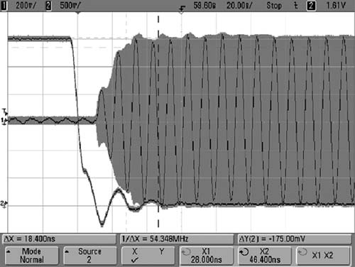
Figure 2 Optimized PHEMT switch process - 90 to 98% RF gate lag time = 18.4 ns.
Figures 1 and 2 present measured gate lag data taken on standard and optimized process/structure PHEMT switches. In Figure 1, it can be seen that a gate lag delay of 274 microseconds was obtained as the switch transitioned from a 90 to a 98 percent level of the RF envelope. With the new PHEMT structure, the data in Figure 2 shows a total gate lag delay at the same 90 to 98 percent level of the RF envelope of only 18.4 nanoseconds. This is an improvement of almost a factor of 15,000 times. In addition, measurements of the 10 to 90 percent RF levels on this FET structure resulted in a switching speed of only seven nanoseconds as compared to a typical 50 nanoseconds on standard PHEMT switches. Combining these two improvements, a total switching speed for a 2 to 98 percent transition of 25 nanoseconds was obtained.

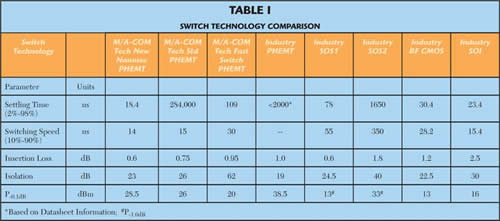
On an absolute level, while the above improvements in the switch settling time and in the overall switching speed are very significant, a comparison relative to similar GaAs PHEMT switches and other semiconductor technologies, which is presented in Table 1, are very revealing. This table was compiled by a combination of data sheet information and direct measurement at M/A-COM Technology Solutions of the settling time and the overall switching speed of specific switches that were felt to be representative of different industry technologies and were purchased through commercially available distribution channels.
If only the GaAs PHEMT switch processes are considered, the settling time for the new nanosecond switch process is truly in a class by itself. When compared to industry standard processes, the new low gate lag switch structure has a settling time that is measured in nanoseconds and compares to the standard processes settling times measured in microseconds or hundreds of microseconds. If the previous "Fast Switch" is used for comparison, the gate lag time of approximately 100 nanoseconds, while much better than standard PHEMT switches, still does not measure up when compared to the new nanosecond PHEMT structure.
Extending the comparison into silicon-based RF switch technologies, Table 1 lists the same switch parameters that were used to characterize all of the GaAs PHEMT devices for Silicon-on-Sapphire (SOS) technology. SOS was pioneered as a technological replacement for standard silicon CMOS by RCA in the early 1970s. The advantages of SOS over standard CMOS included a significant reduction in size, much lower access time, and higher frequency operation when applied to timing circuitry, DRAM memory, and CMOS-based microprocessors. While RCA only exists today as a brand name, other companies have picked up the SOS technology baton and significantly advanced the performance by application of shorter gate lengths, and tighter, more dense design rules, resulting in a true RF capability combined with CMOS logic.
Referencing Table 1, when the new nanosecond GaAs PHEMT technology is compared to two SOS high frequency switches, the settling time is significantly worse for either SOS switch with absolute times for gate lag ranging from tens of nanoseconds to as high as several microseconds. In addition, the standard switching speed to a 90 percent level exhibits similar proportional delays when compared to the new nanosecond PHEMT switch structure. The basic switch parameters shown in Table 1 indicate that the insertion loss of the SOS is generally higher, the isolation comparable, and the typical linearity, P-0.1dB, is significantly worse when measured against the nanosecond GaAs PHEMT technology. In fact, the standard high frequency switch parametric of P-0.1dB for linearity is not even specified, but the much less capable parameter of P-0.1dB is employed.
The last two silicon RF technologies that were compared to the nanosecond PHEMT technology are RF CMOS and Silicon-on-Insulator (SOI), FET-based switches from two different suppliers. Commercially available high frequency switches in both RF†CMOS and SOI technologies have settling times and overall switching speeds that are certainly comparable to the new nanosecond PHEMT switches; however, these silicon RF switches suffer from generally higher insertion loss and severely degraded P-0.1dB linearity. This demonstrates that the new patent pending nanosecond GaAs PHEMT switch process/structure is in a "class by itself" when it comes to overall RF and microwave performance.
References
- A.F. Basile, A. Mazzanti, E. Manzini, G. Verzellesi, C. Canali, R. Pierobon and C. Lanzieri, "Experimental and Numerical Analysis of Gate- and Drain-lag Phenomena in AlGaAs/InGaAs PHEMTs," The 10th IEEE International Symposium on Electron Devices and Optoelectronic Applications, EDMO 2002, pp. 63-68.
- S. Dhar, V.R. Balakrishman, V. Kumar and S. Ghosh, "Determination of Energetic Distribution of Interface States between Gate Metal and Semiconductor in Sub-micron Devices from Current-voltage Characteristics," IEEE Transactions on Electron Devices, Vol. 47, No. 2, February 2000, pp. 282-287.
- A. Freeston, "Understanding Gate Lag and How it Differs From Switching Speed," Microwave Product Digest, September 2008.
