 Base station (BTS) RF front-end design has in the past put more emphasis on performance compared to cost and size. However, to meet the evolving needs of the wireless infrastructure industry, BTS designers today are facing more challenges. Achieving the desired RF performance is only part of the equation for today's BTS RF front-end design. At the same time, cost is also a critical consideration to maintain competitiveness in handling escalating pricing pressure. More channels are now required to fit into a transmit/receive (Tx/Rx) card, which leads to PCB real estate becoming another key factor for BTS designers. In addition, the time to market has condensed, so design cycle time is a critical consideration for BTS RF front-end design.
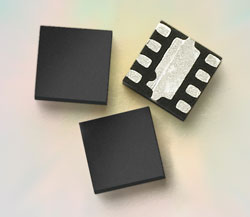
A critical design consideration for BTS receiver RF front-end design is selecting an appropriate low noise amplifier (LNA) to address all the new design challenges mentioned above. With the release of the MGA-633P8 ultra low noise, high linearity active bias low noise amplifier, Avago Technologies has provided an optimal solution. The MGA-633P8 has superior RF performance achieved through the use of the company's proprietary 0.25 μm GaAs enhancement-mode PHEMT process, with an optimum operating frequency range of 450 to 2000 MHz. Similar to Avago's former MGA-631P8 and MGA-632P8 active bias LNA series, the MGA-633P8 is housed in the same industrial standard miniature 2.0 x 2.0 x 0.75 mm surface-mount 8-lead QFN package. The MGA-633P8 is targeted as the single-ended or balanced first-stage LNA for various cellular base station applications, such as transceiver radio cards, tower mounted amplifiers (TMA), combiners, repeaters and remote/digital radio heads.

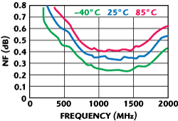
Figure 1 NF vs. frequency at various temperatures.
Receiver sensitivity is one of the most critical requirements for BTS receive path design. This is especially important with the recent development of the wireless infrastructure industry, where providing optimum coverage with the best signal quality is highly desirable. A proper selection of the LNA, in particular the first-stage LNA that greatly affects the BTS receiver sensitivity performance, is required. At 900 MHz, the superior noise figure of 0.37 dB and gain of 18 dB, the MGA-633P8 is one of the best candidates to offer superior receiver sensitivity performance for today's BTS design (see Figure 1). The MGA-633P8 is best suited to both single-ended and balanced configuration applications.

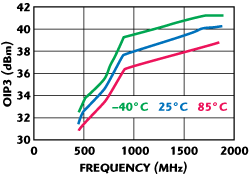
Figure 2 OIP3 vs. frequency at various temperatures.
Another key element for the BTS receiver path design is the linearity requirement, which affects the ability of the receiver to distinguish between the closely spaced wanted and spurious signals. At 900 MHz, typical operating condition of 5 V/54 mA, the MGA-633P8 offers 37 dBm OIP3. With the optimum NF and OIP3, the MGA-633P8 offers enough design margins for the BTS receiver path, especially the first-stage LNA application. Figure 2 shows OIP3 performance versus frequency.
With built-in active bias circuitry, the MGA-633P8 also comes with a current adjustable feature. The Idd current is adjustable by changing the Rbias value. This allows designers to choose between Idd versus OIP3, while maintaining optimum NF. This feature offers BTS designers the flexibility to meet various design requirements and needs with the same product.

Figure 3 Input return loss, output return loss, gain and reversion isolation vs. frequency.

Figure 4 K-factor vs. frequency at various temperatures.
Besides offering the optimized NF and OIP3 performance, the MGA-633P8 also offers input return loss of 15 dB and output return loss of 21 dB at 900 MHz (see Figure 3). Therefore, the MGA-633P8 is easy to use in the BTS design where either an RF filter or attenuator are typically used in the preceding or later stage of a LNA. S-parameters and noise parameters are available to designers who wish to further simulate and optimize the performance based on their specific requirement (see Figure 4).
In addition to optimized RF performance, the MGA-633P8 is equipped with a high Pin absolute maximum rating of +20 dBm. This prevents MGA-633P8 from being damaged by the high input power leaking into the receiver path, particularly a TDD application.

Figure 5 MGA-633P8 application schematic.
As far as application circuitry is concerned, the MGA-633P8 is designed with built-in active bias circuitry, thus eliminating the needs of designing an external active bias network, which is complex and time consuming. The MGA-633P8 is designed with input and output close to 50 ohms. It requires one inductor and one capacitor for both the input and output match. Including DC blocking capacitors, RF bypass capacitors and Rbias, the MGA-633P8 requires nine external components for typical operating conditions (see Figure 5). With a minimum amount of external components count, coupled with a built-in active bias feature, the MGA-633P8 greatly simplifies the design efforts, occupies a minimal amount of PCB space and improves manufacturing yield at the same time.
There are three products in total for this new active bias LNA series, and the upcoming MGA-634P8 and MGA-635P8 (aiming to be released in June of 2010) will be covering 1500 to 2500 MHz and 2300 to 4000 MHz, respectively, thus supporting all major cellular bands for GSM, CDMA, UMTS, WiMAX and next generation LTE bands. Most importantly, all these products will be sharing the same package footprint, Pin/out and external matching network; thus, a common PCB design can be used for BTS designed to operate at different frequency bands. This further adds value to the BTS designs by reducing the PCB layout iterations and is essential for the BTS application with common platform designs.
The key objective of Avago Technologies' Wireless Semiconductor Division is to distinguish customer product with differentiated RF semiconductor technology. With all the key features stated above, the new MGA-633P8 from Avago Technologies has created a distinct value proposition for customer products, and assisting BTS designers to overcome today's BTS design challenges.
Avago Technologies,
San Jose, CA
(800) 235-0312
support@avagotech.com
www.avagotech.com.
RS No. 300
