
In building a strategy for effective integrated-circuit design, it is important to understand the characteristics of different RF and microwave planar dividers/combiners. Optimization of the design process for dividers and combiners can reduce unnecessary costs and design iterations, thus allowing designers time to improve the quality of the product. The design process includes various stages from analysis of requirements to final design documentation, balancing and trading-off factors such as electrical performance, size, cost, etc.
Definitions of Dividers/Combiners
Dividers and combiners are used frequently in RF and microwave integrated circuits as separate components or as parts of devices such as attenuators, phase shifters, mixers, amplifiers, modulators, high power transmitters and beam forming networks for antenna arrays.1 A reciprocal divider can provide an equal or unequal power split between two or more channels. Because of their reciprocity, these circuits may also be employed to combine a number of oscillators or amplifiers to a single port. However, the combining mode has some particularities. To get lossless combining, input signals should be coherent and of equal amplitudes.
The major parameters that define planar RF and microwave dividers/combiners are bandwidth (BW), power division (m), relative output phases (Δφ), phase imbalance, amplitude imbalance, insertion loss (IL), matching (VSWR) or return loss (RL), isolation (ISO), power handling capacity, total number of inputs/outputs, integration level and cost. Insertion loss is the ratio (in decibels) of input power to output power with reflectionless terminations connected to the ports of the divider/combiner. The insertion loss of a printed divider/combiner is a combination of conductor loss, dielectric loss, isolation loss and mismatching loss. The relative phase difference can be quadrature (Δφ = 90°) or in-phase/out-of-phase (Δφ = 0° or 180°). The divider/combiner bandwidth is the range of frequencies for which a parameter falls within a specified limit with respect to certain characteristics.
Dividers/combiners can be classified according to the following performance characteristics:
- narrow band (less than 20 percent) or broadband (greater than 20 percent)
- in-phase/out-of-phase or quadrature outputs
- number of outputs: two, three, four, etc.
- distributed, lumped-element, or combination of both
- equal or unequal power division
- fixed or tunable power division
Planar Divider/Combiner Design Flow and Optimization
Figure 1 illustrates the design flow of a planar divider/combiner. The definition of the system level specification is the first step in the design flow. This involves both the system level requirements, which are applied directly to a divider/combiner, and the derived requirements, which depend on system requirements. Divider/combiner specifications include electrical, cost, size and other requirements. RF specification also includes margin for manufacturing tolerances, environmental conditions and performance degradation over a system’s life.

Figure 1 Planar divider/combiner design flow.
For all requirements, a designer has to choose consecutive integer values of weighting coefficients ki corresponding to each parameter (step 2), with k = 1 for the most important parameter. The maximum value of k can be less than or equal to the number of parameters, depending on whether some parameters are considered to have the same importance or not. Selection of a divider/combiner prototype (step 3) must take into account the corresponding weighting coefficients. The final selection of a divider/combiner prototype can be made by analysis of a circle diagram.2 The optimum prototype should have the minimum area between real and goal performance. For the selected prototype, transmission line (step 4) and technology process (step 5) should be defined. For minimum cost, most dividers/combiners use microstrip lines. However, for lower loss, a stripline or a suspended stripline design is desirable. The design strategy of a printed transmission line type was described previously.2 The type of optimal transmission line depends on many different factors, including the technology process. Sometimes the divider/combiner prototype does not satisfy the requirements. In this case a new modified circuit should be selected (step 9) to satisfy divider/combiner requirements.
The search procedure for the optimum prototype was described in a previous article.2 The synthesis of a planar divider/combiner is based on both system requirements and derived requirements. The synthesis results are the physical dimensions of a divider/combiner and the lumped element values, if necessary. Analysis of a printed divider/combiner entails definition of electrical performance with the known physical dimensions. An electromagnetic simulation may be used to create an S-parameter model for a divider/combiner. Dividers/combiners, symmetrical with respect to one or two planes, are frequently implemented in RF and microwave devices. A mirror-reflection method3 is widely used for analyzing symmetrical networks. In the RF and microwave technique, the analysis of a divider/combiner using matrix representation is very popular. The following procedure of analysis and calculation of a symmetric divider/combiner is recommended:3
- Determine the transfer matrices of the two-port networks (symmetrical parts of a divider/combiner) for both even- and odd-mode excitation. In the case of a cascade connection of two-port networks, the transfer matrix is equal to the product of the transfer matrices of the components
- Determine the most important scattering element of the divider/combiner. For example, let us say it is S11, which characterizes the input matching
- Determine the relationship among admittances (or impedances) of the line segments of the divider/combiner from the condition of perfect matching: S11 = 0
- Calculate the remaining elements of the scattering matrix accounting for the found relationships among admittances
- Determine the characteristics of the divider/combiner
The parameters of the divider/combiner can be simulated using the ADS program. In this case, the designer has to set up variable parameters that can be used to optimize a divider/combiner. Analysis of manufacturing tolerances should be considered to avoid excessive manufacturing cost. For high frequency dividers/combiners, this analysis is especially critical.
Trade-off analysis of a planar divider/combiner includes criteria determined from specifications. The trade-off design includes the following contradictory characteristics: cost vs. tolerances; cost vs. thermal characteristics; cost vs. reliability; cost vs. loss; integration index vs. cost; integration index vs. tolerances; size vs. Q-factor; size vs. tolerances; size vs. maximum power; bandwidth vs. amplitude balance and quantity of sections. The principal trade-off is between frequency range, insertion loss and amplitude balance. The most contradictory requirements are size vs. loss. The integration quality of the divider/combiner is characterized by the following parameters: volume V (inches or centimeters cubed), minimum of dissipated losses A0 (in dB) within the bandwidth, bandwidth (Δf / f0) in percent and the number of sections. The relationship between these controversial parameters is described by the integration index.3
The final documentation (step 8) of the optimized planar divider/combiner should include the following issues:
- Type of planar divider/combiner
- Main performance: frequency range, bandwidth, power split, isolation, impedance, return loss, insertion loss, maximum power, relative phase difference between output signals, phase and amplitude imbalance
- Drawing with physical dimensions
- Technology process used
- Packaging (package material, technology process, hermetic or non-hermetic, housing physical dimensions)
- Tolerance analysis results
- Thermal analysis results
- Reliability analysis results
- Cost analysis
Types of Planar Dividers/Combiners
More than 100 different types of power dividers/combiners have been developed over the past four decades, often in quest of additional bandwidth, lower loss, smaller size, greater isolation, or other performance advantages. In this section, the main types of planar dividers/combiners and their modifications are considered. The main four types of planar dividers/combiners include (see Figure 2):
- T- and Y-junction circuits
- resistive three-port circuits
- Wilkinson dividers/combiners
- four-port circuits based on directional couplers

Figure 2 The four main types of planar dividers/combiners.
The simplest planar three-port divider is analogous to coax and waveguide T-junction. To improve the matching, the lines can be connected at 120° to each other. Circuits connected in this way are called Y-junctions. T- and Y-junctions can have a series or a parallel connection of one input and two outputs. In a series planar connection, the signal splits out of phase; in a parallel connection, it splits in-phase between two outputs. The simple three-port network structure of T- and Y-junctions has two significant drawbacks: the absence of isolation between output ports and the imperfect matching of all ports. A lossless, reciprocal three-port circuit can be physically matched at only two ports. In the transmit direction, the divider input has an excellent VSWR, typically less than 1.15:1. In the receive direction (combiner mode), the VSWR is not as good. Microstrip T- and Y-junctions are shown in Figures 3a and 3b. The T-junction of three slotlines is displayed in Figure 3c. Figure 3d shows the coplanar waveguide T-junction for an in-phase power divider.

Figure 3 Simple three-port networks: (a) T-junction, (b) Y-junction, (c) T-slotline junction and (d) T-coplanar waveguide junction.
The basic structures of a resistive three-port divider are shown in Figure 4. One version has resistors in the form of a star (or “wye”) (see Figure 4a); the other is in the form of a delta (see Figure 4b). The resistive three-port divider can be matched at all ports. The given resistor values will ensure that each port is impedance matched to Z0. Any mismatching on one output will be reflected to the other output. The resistive power divider can work over many octaves. In fact, there are commercially available resistive dividers that cover DC to 40 GHz. In addition to their broad frequency range, they are very compact because they include only lumped elements. The resistive power divider suffers some serious drawbacks. In the resistive divider, half of the input power is dissipated. Another disadvantage is the lack of isolation between output ports. Even though it is not lossless, isolation is still not achieved. The isolation of a resistive divider is equal to its insertion loss (6 dB). Also, the problem with the resistive divider/combiner is the power-handling capability of the internal balancing resistor.
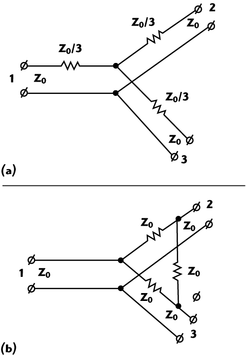
Figure 4 Resistive three-port dividers: (a) star and (b) delta.
N-way resistive dividers can be easily developed from the star divider. The appropriate resistors for an N-port star divider are found by the equation:
For example, a three-way divider needs resistors of Z0/2, while a four-way divider needs resistors of 3Z0/5 and so on.
The Wilkinson divider (see Figure 5)3-5 provides matching of all three ports, low loss, in-phase split and high isolation between output ports. The Wilkinson divider/combiner has a small resistor that limits its ability to combine any signals of higher power than that of the resistor, which is rated for several watts. Perfect matching of all divider ports and perfect isolation between output divider ports are obtained if

where R2 is the resistance of the lumped element resistor; Y1=Z0/Z1 is the normalized admittance of line segment of length l; z0 is the characteristic impedance of the input /output port lines; Y2=2z0/R2 is twice the normalized admittance of resistor R2.

Figure 5 Wilkinson dividers/combiners.
As opposed to the reciprocal T- or Y-junction, the Wilkinson divider can be matched at all ports simultaneously because this three-port circuit uses a lossy element (resistor R2). The Wilkinson divider is a network with outputs whose phase relationship is 0°. The real divider characteristics deviate from the ideal, due to manufacture tolerances, losses, discontinuities, and mismatching of terminations, as well as the physical quality of the resistor. The influence of these different factors on the parameters of the divider was examined by Paral and Moynihan.3 For combining two or more oscillators, the Wilkinson combiner sometimes requires specified isolation between input ports to provide mutual synchronization between oscillators.3 Such a combiner with specified oscillation between ports 1 and 2 can be realized (see Figure 5b) with a variable resistor. The isolation value for this network is
For perfect matching of ports 1 and 2, it is necessary that:
![]()
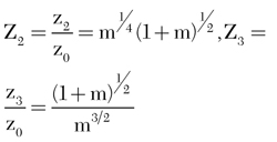
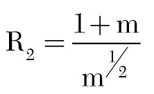
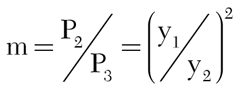
The Wilkinson divider with unequal power-split ratio m=P1/P2≠1 (see Figure 5c)3,4,6 consists of two quarter-wave segments 1-2 and 1-3 of different impedances
and lumped resistor:
Due to the quarter-wave length segments, the Wilkinson divider bandwidth is limited to approximately 20 percent. Some applications require broadband Wilkinson dividers. Figure 5d illustrates the broadband version of a narrow band cascading of the Wilkinson power divider. Each section must have quarter-wave segments of different characteristic impedance, and each resistor must have a different value. The two-section divider has an octave bandwidth. It is possible to build a broadband divider from 2 to 18 GHz using more than two sections. As a general rule, the greater the bandwidth the more sections are added to the design. However, as the number of sections increases, the insertion loss and the complexity of the device also increase.
Another broadband resistive divider/combiner is based on coupled transmission lines.3,7,8 The simplest version of the coupled transmission line two-way power divider/combiner is shown in Figure 5e.8 It consists of two identical quarter-wavelength coupled lines positioned with respect to common ground, load resistor RL and isolating resistor Ri.
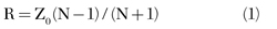
Dividers/combiners with more than two inputs/outputs are used in antenna arrays, in combining networks, etc. A three-way Wilkinson divider/combiner with “star-resistor” configuration is shown in Figure 5f. The arms have an impedance of √3 Z0 and the resistor value is equal to the input impedance. Figure 5g shows a three-way Wilkinson divider/combiner with the “delta” resistor configuration. The arms again have an impedance of √3 Z0, but now the resistors have an impedance of 3Z0. A disadvantage of an N-way (N>2) divider/combiner is the fact that this network requires crossovers for the lumped element resistors that makes fabrication difficult in planar implementation.
A directional coupler is a reciprocal four-port circuit, which provides two different amplitude outputs when a signal is applied to its input. This definition of a directional coupler suggests its possible use for splitting power from one port between two other ports. The dividers and the combiners based on the ring directional coupler are shown in Figure 6. A matched ballast termination R4 (see Figure 6a) is “ballast” only from the structural point of view. The admittances of the ring power divider/combiner are3

where
is the power split ratio of the ring divider.
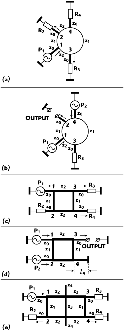
Figure 6 Directional couplers used as divider/combiner.
The divider and the combiner based on a two-branch directional coupler are shown in Figures 6c and 6d, respectively. The normalized admittances are
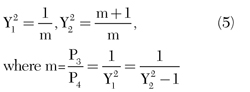
From Equations 1 and 2, the admittances of ring and two-branch dividers can be determined. For m > 3, it is difficult to realize the corresponding ratio of admittances; therefore, the maximum practical power split used is m = 3. The main advantage of the quadrature hybrid is to isolate the input port from its two outputs if the load’s VSWR, magnitude and phase of reflection signals are identical. That is why the quadrature-combined circuit appears to be well-matched.
In the circuit shown in Figure 6d, equal quadrature signals of two identical-frequency oscillators connected to ports 1 and 2 of a 3 dB two-branch coupler are combined. In the ideal case, the combined power appears only on port 3, while port 4 is isolated. If conditions of equal power, phase quadrature and equal frequencies are not satisfied, then an unbalanced signal appears on port 4. Due to a specially introduced mismatching element (short or open segments l4 of adjustable length), the unbalanced signal is reflected from the end of line l4 and travels into the two oscillators for mutual synchronization. In some applications, coherent addition of signals is not a requirement; for example, where n signals of different frequencies are applied to a device with a single output port (multiplexer).
The three-branch divider with power split regulation is shown in Figure 6e. Two reactances (open or short stubs) are connected to the center branch. If port 1 (or port 3) is the input, the power split between ports 2 and 4 depends on the stub length. For perfect matching at the mid-frequency band, the normalized characteristic admittances Y1, Y2 and Y3 are given as

The dividers/combiners based on directional couplers have an advantage over T- and Y-junctions: the split power ratio m is proportional to the square of the ratio of admittances, which gives more room for increasing m. However, a decrease in admittance and a corresponding decrease in the width of the conductor of the microstrip line lead to increased losses. The branch-line dividers/combiners are effective for planar fabrication of balanced circuits because the output ports of the network are on the same side.
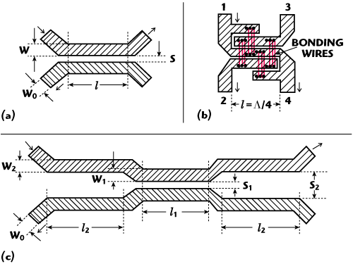
Figure 7 Coupled-line directional couplers.
A coupled-line directional coupler (see Figure 7) can be used for broadband power division or combining. The planar edge-coupled-line coupler cannot be implemented for a power division m < 10 because of etching tolerances. The 3 dB broadband Lange directional coupler (see Figure 7b) is used for equal power division (m = 1). The divider based on the single-section coupled line directional coupler is limited in bandwidth due to the quarter-wave length section. Bandwidth can be increased by using multiple sections (see Figure 7c). The disadvantage of couplers used for dividers or combiners is the complexity of the circuit. The advantages of these couplers are convenience of adjustment and good electrical characteristics.

Figure 8 Lumped element Wilkinson dividers.
Consider lumped-element dividers/combiners. Choosing between distributed-element and lumped-element designs depends on several factors.9 Some of these include size, insertion loss, frequency and cost. For example, lower-frequency RF components are often based on lumped-element components. Higher-frequency designs (2 to 30 GHz) can use distributed elements. The distributed Wilkinson divider and dividers based on directional couplers can be converted into the lumped element π network (see Figure 8). For the center frequency f0, the quarter-wavelength segment with characteristic impedance z has the π-section lumped element equivalent with series inductance L, as well as two shunt capacitances C3 with the following values:
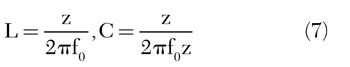
Figure 8b illustrates the lumped element Wilkinson divider. A lumped-element layout is much smaller than the distributed layout (see Figure 5a). For this example, the π arrangement was chosen to reduce the number of lossy inductors as compared to the T-equivalent.3 The input shunt capacitors (port 3) are combined into a single capacitor yielding two inductors, one shunt capacitor at each port, and the 100 Ω isolation resistor. The bandwidth of a lumped-element Wilkinson divider is approximately half that of the microstrip distributed version.
Figure 8c shows the lumped element divider based on the two-branch directional coupler.10,11 The bandwidth performance of this divider is narrower, due to parasitic elements in the models of capacitors and inductors. Table 1 compares the performance of different dividers/combiners.

The major differences between using the Wilkinson divider/combiner versus the branch-line hybrid is that the input match of the Wilkinson circuit depends on the match at the other two ports. However, it is much easier to get wider bandwidth with the Wilkinson divider/combiner than with the two-branch circuit. Choosing between the divider based on the directional coupler or on the Wilkinson circuit is a matter of the power levels of input/output signals. Wilkinson dividers have small resistors mounted on PCB, which limits their ability to operate with signals higher than the value of the resistor power. The divider based on directional couplers has external loads to absorb power, so it is applicable to powers of several hundred watts. The power split m ≥ 3 is difficult to realize in the resistive three-port dividers and dividers based on the ring and branch-line directional couplers. The limiting factor here is the impossibility of manufacturing narrow printed conductors of high impedance segments.
Figure 9 shows an example of the design flow for the selection of a planar divider prototype. In this example, the divider requirements and their weighting coefficients include: the frequency range is L-band with the weighting coefficient of the highest importance (k1 = 1); 30 percent bandwidth with the weighting coefficient of the highest importance (k2 = 1); the total number of outputs = two, with the weighting coefficient k3 = 1 of the highest importance; the isolation between outputs at 20 dB, with the most important weighting coefficient k4 = 1; power ratio m = 1 with the most important weighting coefficient k5 = 1; minimum size with the weighting coefficient k6 = 2; minimum cost with the weighting coefficient k7 = 3. The selection of a directional coupler prototype starts with satisfying the most critical requirements with weighting coefficients k1 = k2 = k3 = k4 = k5 = 1 (step 3.1, 3.2, 3.3, 3.4, 3.5), and then the less critical requirements with k6 = 2 (step 3.6) and k7 = 3 (step 3.7). The design flow shows that the optimum divider prototype for the above specifications is the simple Wilkinson divider (see Figure 5a).
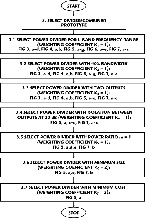
Figure 9 Design flow for selection of a planar divider.
Applications of Dividers/Combiners
Figure 10 illustrates different configurations of a reflection-type phase shifter. In the phase shifter shown in Figure 10a, the two output ports are terminated with voltage variable capacitors to ground. The divider splits the input signal of equal amplitude with a phase difference of 90°. Then the signals are reflected from the capacitors back to the hybrid and combined at the output port 2. If the magnitudes and angles of reflection signals are equal, there will be two reflection signals that are equal in amplitude and in phase quadrature. These signals will combine at the isolated port 2 and will cancel at the input port 1. This reflection-type phase shifter provides a voltage variable phase shift between 0º and close to -180º. The power divider including the two-branch divider/combiner and two reflected loads with shunt diodes D1 and D2 is shown in Figure 10b.3,4 An input signal is divided by the quadrature divider among the two ports. The diodes are biased in the same state (forward or reverse biased). The input signal is divided into two quadrature components with equal amplitudes on the output ports. Turning the diodes ON or OFF changes the total path length for both reflected waves by Δφ, producing a phase shift of Δφ at output 2. Figure 10c illustrates a reflection-type phase shifter using a divider/combiner based on the Lange coupler and varactor diodes D1 and D2. The ideal varactor diode is a variable capacitor with the capacitance value changing as a function of the DC bias.

Figure 10 Reflection-type phase shifters.
Figure 11 illustrates different combiner circuits based on directional couplers. The chain structure of the combiner of Figure 11a includes the series connection of three ring directional couplers. The couplers are connected by connecting lines between one output/input of one divider/combiner with one input/output of the next divider/combiner. This network can be used as a combiner of four oscillators.3 The characteristic impedances of the different ring segments are determined in accordance with the oscillator power ratio. The network of Figure 11b ensures the power combining of four oscillators using three two-branch couplers. Adjustable segments (short or open lines with variable length) provides mutual coupling between oscillators to implement mutual synchronization between oscillators.3 The schematic of a 3:1 combiner (see Figure 11c), including a network of 3.0 dB and 4.77 dB couplers, provides 4.8 dB loss in each signal path (33 percent split). Due to losses in the three-way combiner, higher coupler values, such as 5.0 dB, are actually better suited for this function.
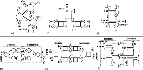
Figure 11 Combiner circuits using directional couplers.
Different balanced amplifier schematics with power dividers/combiners are shown in Figures 11d, e and f. The use of splitting and combining in the balanced amplifiers comes from the need to replace one high power amplifier with two or more less expensive amplifiers. Figure 11d illustrates a balanced power amplifier including a four-way divider, a four-way combiner and four low power amplifiers. The input divider and the output combiner use Wilkinson dividers/combiners. The input divider splits the input power equally between the four output ports. The output combiner recombines the output signals from the amplifiers. To minimize balance differences between the splitting and the combining circuits, the same circuits can be used for both functions. The most important parameter of this circuit is the power loss after amplification. The loss of actual dividers/combiners differs from the ideal, due to the mismatching of all ports, transmission line loss, discontinuities, as well as manufacture tolerances.
Another form of circuit loss is defocusing, which can be defined as the amount of power that is directed to circuit termination instead of to the circuit output port (see Figure 11e). This power is directed to termination R due to amplitude and phase balance errors introduced by the dividers/combiners and the amplifiers. The main advantage of the quadrature hybrid of Figure 11e is the isolation of the input port from its two outputs, if the load’s VSWR, magnitude and phase of the reflected signals are identical. The power amplifier chain structure with three amplifiers (see Figure 11f) includes a three-way divider consisting of a 3 dB coupled line coupler, a 4.77 dB coupled line coupler, and a combiner consisting of a 4.77 dB coupler and a 3 dB coupler. The electrical parameters of the three-way divider and combiner should have very strong magnitude and phase relationships between the three channels in order to provide a high PA efficiency. Also, the insertion loss of the divider and combiner is very critical. For the 4.77 dB coupler of the divider, the voltage transfer coefficients3 are
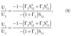
where Γ2,Γ3 are the reflection coefficients of the coupler loads in port 2 and port 3, respectively.
The conventional RF eight-port beam forming network based on four hybrid dividers/combiners is used for determining both azimuth and elevation information in monopulse radar systems. The monopulse networks (see Figure 12) provide connection of four inputs/outputs 1, 2, 3 and 4 to output/input ports 5, 6, 7 and 8, which can be connected to four antenna elements. These eight-port hybrid matrices provide equal amplitudes and specific relative phases for the four antenna monopoles to form the directional antenna pattern.12 Figure 12a illustrates a Butler matrix,13 including four two-branch hybrids H1, H2, H3, H4 and two 45° phase shifters. Four antenna elements connected to ports 5, 6, 7 and 8 provide four antenna beams in the desired directions.

Figure 12 Monopulse networks.
The amplitude monopulse network (see Figure 12b)12 includes four dividers/combiners and a switched 0°/180° phase shifter, connected in series. This 4 x 4 matrix should be asymmetrical to take into account the losses of the switched phase shifter to provide an amplitude balance at all four antenna terminals 5, 6, 7 and 8. Therefore, hybrids H1, H2 and H4 should have unequal power ratio m (see Equation 2), depending on the phase shifter loss. The direct connection of the four two-branch hybrids (without an additional connection line between them) makes the bandwidth of the 4 x 4 matrix slightly narrower than the bandwidth of the single two-branch hybrid due to undesirable interaction between the four hybrids. When the four hybrids H1, H2, H3 and H3 are connected using quarter-wavelength transmission lines (invertors I1, I2, I3 and I4) (see Figure 12b), the quality of the circuit is improved.12 Figure 12c illustrates a monopulse comparator circuit using dividers/combiners based on the 0º/180º hybrid rings. If the four input ports with signals A, B, C and D are connected to four antenna elements, the output signal (C+D) - (A+B) is proportional to the elevation angle and the output signal (B+D) - (A+C) is proportional to the azimuth angle.
Acknowledgment
The author would like to thank Dr. S. London for his helpful remarks.
References
1. G.L. Matthaei, L. Young and E.M.T. Jones, Microwave Filters, Impedance Matching Networks and Coupling Structures, Artech House Inc., Norwood, MA, 1980.
2. L.G. Maloratsky, “Setting Strategies for Transmission Lines,” Microwaves & RF, September 2008, pp. 100, 102, 104-112; October 2008, pp. 84, 86.
3. L.G. Maloratsky, Passive RF & Microwave Integrated Circuits, Elsevier, Burlington, MA, 2003.
4. M.D. Pazar, Microwave Engineering, Second Edition, John Wiley & Sons Inc., Somerset, NJ, 1998.
5. E.J. Wilkinson, “An N-way Hybrid Power Divider,” IRE Transactions on Microwave Theory and Techniques, Vol. 8, No. 1, January 1960, pp. 116-118.
6. L.I. Parad and R.L. Moynihan, “Split-tee Power Divider,” IEEE Transactions on Microwave Theory and Techniques, Vol. 3, No. 1, January 1965, pp. 91-95.
7. S.Y. London, “A New Broadband Coupled-line N-way Power Combiner/Splitter,” Applied Microwave & Wireless, May 2001, pp. 28, 30, 32, 34, 36, 37, 38.
8. L.G. Maloratsky and S.Y. London, “Quarter-wavelength N-way Power Dividers/Combiners: Historical Aspects and New Modifications,” Microwave Journal, Vol. 46, No. 9, September 2003, pp. 194-202.
9. J.E. Penn, “Convert Distributed MICs to MMICs,” Texas Instruments, June 2003.
10. A. Grebennikov, “Power Combiners, Impedance Transformers and Directional Couplers: Part III,” High Frequency Electronics, February 2008, pp. 42, 44, 46-48, 50-52.
11. M. Burdick, et al., “Splitters/Combiners Team with RF LDMOS in UMTS Amp,” Microwaves & RF, July 1999, pp. 80, 83, 85, 86, 88, 90, 92.
12. L.G. Maloratsky, “Analyze Bearing Accuracy of a Monopulse System,” Microwaves & RF, March 2009, pp. 61, 62, 64, 65, 66, 67.
13. J. Butler and R. Lowe, “Beam Forming Matrix Simplifies Design of Electronically Scanner Antennas,” Electronic Design, April 1961, pp. 170-173.
Leo G. Maloratsky received his MSEE degree from the Moscow Aviation Institute and his PhD degree from the Moscow Institute of Communications in 1962 and 1967, respectively. From 1962 to 1992, he was involved in the research, development and production of RF and microwave integrated circuits at the Electrotechnical Institute and was an assistant professor at the Moscow Institute of Radioelectronics. From 1992 to 1997, he was a staff engineer at Allied Signal. From 1997 to 2008, he was a principal engineer at Rockwell Collins, where he worked on RF and microwave integrated circuits for avionics systems. He joined Aerospace Electronics Co. in 2008.