
Major advances in microwave device development in recent years have enabled a transition to solid-state power amplifiers (SSPA) for wireless communications and radar systems in microwave to millimeter-wave bands. In particular, SSPAs are rapidly replacing electronic tube amplifiers, such as magnetron and traveling-wave tube-based amplifiers (TWTA), for base stations of mobile phones using L- and S-band, and for satellite communications and base stations for terrestrial communications at C- to Ku-band frequencies.
The advantages of SSPA include: 1) the ability to reduce size and weight of devices including the power supply; 2) the ability to reduce spurious signals; and 3) longer-life than electronic tubes (even though technology advances have recently extended the life of tube-based amplifiers). With the spread of multi-carrier modulation and growing requirements for high capacity digital data communications, there has been strong demand for higher power amplifiers, as well as lower distortion for communications applications (see Figure 1).

Figure 1 Demand for higher power FETs for communication equipment.
Higher power amplifiers are in demand for radar systems as well, to expand the detectable range, improve detection of smaller targets and meet electronic countermeasure (ECM) requirements. Moreover, downsizing of power amplifiers has been expected yearly for both communications and radar systems applications to improve mobility and portability, and to relax installation and mounting conditions (see Figure 2).

Figure 2 Demand for higher power in radar applications.
To address these trends and continue to expand communications applications for SSPAs, further advances are needed to take advantage of GaN’s merits to downsize the equipment and obtain higher output power. This article summarizes the development status of GaN devices, which are expected to further expand SSPA applications in microwave and millimeter-wave bands, due to the outstanding GaN material characteristics.
Why GaN?
Until now, GaAs FETs have typically been used for microwave high power amplifiers. As an example, Toshiba Corp. has commercialized C-band 90 W GaAs FET and X-/Ku-band 30 W GaAs FET technology. However, after 30 years of development, the output power of GaAs FET technology is now reaching its physical limits. Practical manufacturing of much higher power FETs than those currently available is facing significant technical difficulties.
Wide Band Gap (WBG) semiconductors have recently been noted as potential alternatives to GaAs devices. Making use of a large band-gap material enables high power operation with high breakdown voltage. As one WBG solution, GaN has those characteristics and features several other benefits: 1) creation of a HEMT (high electron mobility transistor) structure is relatively easy; 2) its electron saturation velocity is high and capable of high frequency operation; 3) among the WBG alternatives, GaN is easier to work with; and 4) it can share production processes with GaAs. As a result of these characteristics, GaN is a prime candidate for the next-generation of higher power devices. Table 1 and Figure 3 show the GaN material constants and features, and compare them to other major semiconductor materials.


Figure 3 Features of GaN material.
Due to a process similar to the GaAs devices shown in items 1) and 3) above, the realization of the HEMT structure shown in Figure 4 is a big advantage for GaN, compared to other potential WBG alternate materials from a practical application standpoint. Compared to GaAs HEMT, GaN has a wider bandgap, and also has a higher 2D electron density that is capable of larger current output as a result of spontaneous polarization/piezoelectric polarization effects.
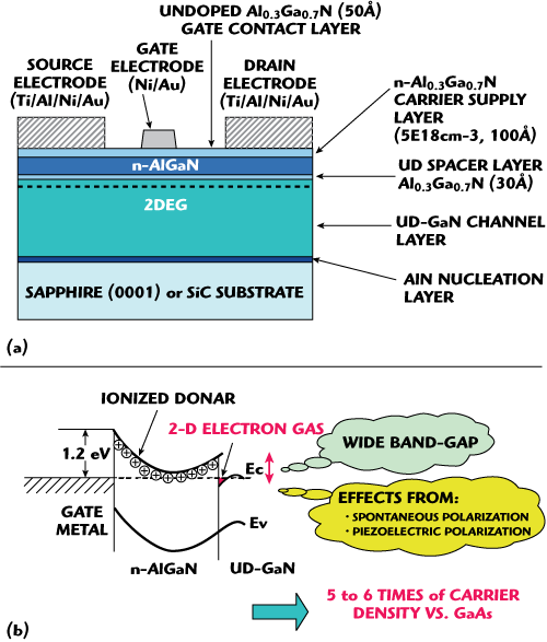
Figure 4 Example of a GaN HEMT structure (a) and a band structure model (b).
The features of GaN in an electronic device include:
- Wide bandgap = High breakdown voltage
- Piezoelectric effect = High electron density → capable of higher power output
- High saturation velocity = Faster and higher-frequency operation
- High thermal conductivity (2.6 times of GaAs) = Capable of higher power output
- Strong inter-atomic bonding power = Stable mechanically and chemically
- High frequency, high power amplifier from L-band to millimeter-waves
- Withstands high temperature, high radiation = Environmentally-resistant devices
- Low-loss power devices
Comparison data of the output power per gate width in transistor units between existing Si-/GaAs- and GaN HEMT can be seen in Figure 5, which indicates GaN’s capability for high power output.
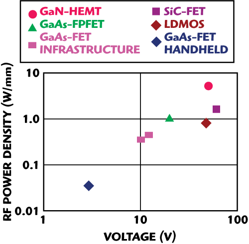
Figure 5 RF power density for high frequency semiconductors.
Progress in GaN Device Development
Research and development on GaN devices began in the mid-1990s. In 2006, 200 W-class devices in the L-/S-band for mobile phone base stations were produced; in 2009, 50 W-class devices in X-band for satellite communications base station and radar use were commercially available. The released research and development reports are summarized here.
L-/S-band (0.5 to 4 GHz)
This frequency band is used primarily for mobile phones, WiMAX or airport surveillance radar. The gain achieved to date with GaN devices is suitable in this band, and some manufacturers have reported output power of over 200 W in pulse-mode operation. Figure 6 shows the photograph and Pin/Pout characteristics1 of an S-band, 800 W-class GaN HEMT released from Eudyna Device Co. Ltd. An output power of 851 W and a drain efficiency of 57.4 percent were reported at 2.9 GHz, with a 200 μs pulse width, a 10 percent duty cycle and 65 V drain-source voltage (Vds) supply.

Figure 6 800 W S-band GaN HEMT from Eudyna.1
C-band (4 to 8 GHz)
Satellite communications, FWA, Wireless LAN, weather radar, etc., are widely used in this frequency band. There has been great interest in replacing electron tube amplifiers with SSPA in these applications. Recently, over 200 W devices in pulse-mode operation have been reported as the result of process and quality improvement of GaN crystals. Figure 7 shows an example of characteristics released in 2005 by Toshiba Corp.: 174 W output power and PAE of 34.7 percent (approximately 43 percent of drain efficiency) were obtained at 6 GHz, with a 20 μs pulse width, 2.5 percent duty cycle, and a Vds = 25 V supply.2 At present, Toshiba has successfully obtained 200 W at 6 GHz by improving the crystal material and process. In addition, a 220 W device, with approximately a 38 percent PAE at C-band with a 20 μs pulse width, a 10 percent duty cycle and a 60 V Vds supply, was also reported by Mitsubishi Electric Co. Ltd. in 2006.3
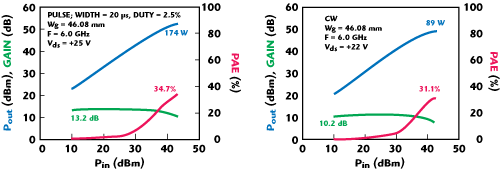
Figure 7 C-band GaN HEMT from Toshiba.
X-band (8 to 12 GHz)
This frequency band is used for satellite communications, earth observation satellites and various radar systems. As the frequency increases, it becomes more difficult to obtain higher gain. To solve this challenge requires refinement of the device structure. Although GaN has a higher breakdown electric field as a material, refinement of the device itself, such as the electrodes, increases the electrical field of its components. As a result, it is more difficult to obtain high power output with more than 50 V of operating voltage than has been possible with devices at C- and lower bands. That is one of the reasons that practical devices operating above 10 GHz have been rarely reported so far.
Figure 8 shows a photograph and the characteristics of an X-band GaN HEMT that Toshiba developed in 2006.4,5 Toshiba achieved 81.3 W output power in continuous wave (CW) operation and a PAE of 34 percent at 9.5 GHz, with a Vds = 30 V supply. X-band power GaN HEMTs in the 50 W-class have also been produced and shipped in the market for over a year.

Figure 8 50 W X-band GaN HEMT: (a) photograph and (b) RF performance.
Ku-band (12 to 18 GHz)
This frequency band is used for satellite communications, satellite television and related applications. However, continued growth of data capacity in recent years is expected to shift additional communications to Ku-band. C-band had also been used for satellite communications with the benefit of lower rain-fading factor in many tropical countries. However, the use of Ku-band satellite communications in those countries has been increasing, despite the drawback of rain-fading. The availability of portable VSAT terminals at Ku-band with small antennas drives this trend.
Refining device structures at Ku-band is harder than it is for the lower X-band frequency. Additionally, some problems have been encountered with heat radiation and in maintaining the breakdown voltage and high-frequency characteristics. Moreover, depending on the device package size, the wavelength becomes nearly equal to the cavity resonance, or the wavelength passing through the package. The cavity resonance frequency must be maintained at a higher level than the operating frequency of the device. Therefore, the size of the package, especially its width, is severely restricted and the technical requirements to obtain higher power become more challenging. Due to such restrictions, GaAs devices are thought to have an output power limit of approximately 30 W. In contrast, GaN has the capability to achieve power output three to five times that of GaAs devices, even under various restrictions, as a result of its material characteristics. Figure 9 shows a photograph of a Ku-band GaN HEMT and its characteristics.6,7 It employs the same package as the X-band GaN HEMT (21.0 x 12.9 mm) and has two GaN HEMT chips mounted inside. The device obtained 65 W output power in CW operation and a PAE of 19.5 percent at 14.5 GHz, with a Vds = 30 V supply.
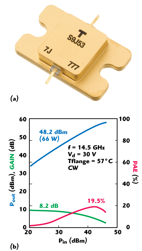
Figure 9 Ku-band 50 W AlGaN/GaN HEMT: (a) photograph and (b) RF performance.
Above K-band (18 to 26 GHz)
This frequency band is for the next-generation satellite communications, to deal with larger data capacity. As mentioned previously, the technical challenge is much higher at high frequencies than at lower bands and no practical devices have yet appeared. Ongoing R&D to address these challenges is centered at various research institutions throughout the world. A report that an output power of 20 W was achieved at 26 GHz was issued from the Research & Development Association for Future Electron Devices.8 This has raised the industry’s expectations for practical devices in the near future.
Benchmark
Figure 10 indicates the development status of cutting-edge GaN HEMT high power devices, based on the released data found. From this summary, it is known that 100 W-class devices up to Ku-band are already commercially available.
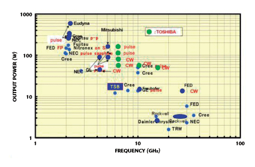
Figure 10 Development status of GaN HEMTs.
Reliability and Future Issues
Current Reliability
Improvements in crystal substrate quality and progress in developing process techniques have made GaN devices more reliable in recent years. As a result, practical devices have now been brought to market. Recently a device that can operate for 100 years or more at 200°C channel temperature has been reported9 and ongoing testing is confirming the reliability of GaN devices. Research into factors concerning device lifetime is ongoing on material and device structures, and correlation between manufacturing process and long life is also being confirmed.10 GaN has not yet been widely employed in many practical uses as a semiconductor device, and some unexpected failure modes may occur that have not yet been anticipated. However, the lifetimes estimated by accelerated testing during manufacturing have now reached an acceptable level.
Future Issues
Quality and Price of Crystal Substrate
As mentioned earlier, the crystal substrate for GaN devices has been improved significantly over the past several years. However, it still requires further refinement, and there is much room to improve the substrate to levels comparable to that of Si and GaAs. The characteristics of GaN/SiC HEMT structures fabricated by an epitaxial growing method can be easily influenced by the crystal quality of GaN or AlGaN layers growing on SiC. Surface defects, which can be observed with a microscope, have been shown to influence device characteristics and reliability,11 but have not been completely eliminated so far. Established techniques to grow defect-free crystals will be required as soon as possible to achieve improvements of GaN device characteristics and a corresponding reduction in price.
Figure 11 shows the relationship between surface defects on the wafer and their influence on the device characteristics.11 As shown in the photograph at the left lower part of the figure, some defects were observed by microscope on the surface of the wafer, and the devices composed on them apparently show differences in electrical characteristics from those on a defect-free part, referring to the graph in the right upper portion of the figure.
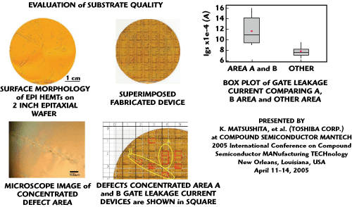
Figure 11 Surface defects on GaN HEMT wafer and their effects on device characteristics.
Current Collapse
Current collapse is a unique phenomenon of GaN-based devices, in which the drain current starts to decrease beyond a certain relatively higher drain voltage with a certain fixed gate voltage. This effect has also been seen on GaN HEMTs fabricated on defect-free parts of the wafer (see Figure 12). Although the mechanism of the current collapse has not been thoroughly clarified, researchers have determined that current collapse is related to defect levels at the boundary between the GaN and SiC in a GaN/SiC structure, on the surface of the GaN crystal near the gate electrode, or on the boundary between GaN and the topcoat. For the products now on the market, current collapse has been suppressed to a level suitable for practical use. If it can be suppressed completely, the characteristics and reliability of the device will be improved even more. Research is ongoing at many companies and universities, in an effort to solve this problem associated with GaN devices.

Figure 12 Example of current collapse.
Measures for Heat Radiation
Development of high power GaN HEMTs has progressed rapidly, taking advantage of GaN’s material characteristics. The power added efficiency (PAE) levels of GaN HEMTs are estimated as approximately the same as GaAs devices. As a result, the power density and output power are higher than GaAs devices, which make the heat density higher as well. Consequently, increasing the PAE of the chip itself and developing techniques to effectively cool the device will be needed to achieve the full power of GaN HEMTs.
Figure 13 compares the heat density of the existing commercial devices and equipment. If the potential of the GaN devices is increased to the highest level possible with current techniques, the heat density may exceed that of a Pentium4®‚ processor. To maximize the GaN’s potential, every measure to effectively cool the device should be considered.
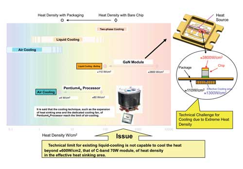
Figure 13 Heat density of the devices and equipment.
Forecast and Examples of SSPA Applications
Forecast
As mentioned throughout the preceding descriptions, the market seems to be cautious to employ GaN HEMT, due to its unknown technical aspects, in spite of high expectations for the eventual development of higher power devices. More specifically, the high potential of GaN to achieve 10 times the power output of GaAs devices will also cause 10 times the heat. This will require special techniques to deal with the thermal issues. However, the degree to which this is a problem depends on the application. For example, the issue of heat dissipation is not as important in radar use because of its pulse operation.
Eudyna Devices Inc. released the kW-class palette amplifier at S-band last year.12 It outputs 1000 W at 3.2 GHz with an 80 Vds supply, 200 μs pulse width and 10 percent duty cycle, with a drain efficiency of 49.5 percent. This indicates that the heat challenges of GaN can be worked through at a high level in pulse operation.
As mentioned in the Ku-band section, the package size has restriction in applications above X-band because of cavity resonance. This is also the reason why the technical limit of GaAs devices on Ku-band is currently said to be 30 W. Yet, this package seems to have capability for up to twice the heat density of GaAs, even with ordinary cooling methods. Therefore, it can be said that a 60 W GaN device in CW operation at X-/Ku-band is realizable, by designing it to achieve twice the power density of GaAs. At this level of power output, the heat problem is manageable.
Radar Applications
SSPA have gathered high expectations as potential replacements for radar transmitters using magnetron and klystron tubes because of their increased reliability. This has become even more important because of limited availability of the electronic tubes. Using GaAs, replacement of electronic tubes by SSPA has been ongoing for transmitters at microwave frequencies (up to C-band), but it has not been practical with GaAs to achieve high power SSPA above C-band. However, GaN devices are now becoming available for pulse-operated applications that take advantage of the new material’s potential. Figure 14 shows a photograph and an example of the characteristics13 of the high power amplifier developed for a X-band weather radar, using a X-band GaN HEMT shown in Figure 8. It delivers over 250 W of output power in the range of 9.1 to 9.6 GHz with at least 38 dB gain and a PAE of 21 percent. Figure 15 shows a photograph of a GaN SSPA transmitter for radar that uses GaN HEMT amplifiers and a photo of the weather radar using that amplifier.14 SSPAs, with semiconductor devices mounted in the transmitting section, have successfully reduced the equipment size to one sixth of that of the existing equipment, using electronic tubes. The equipment has been in operation since the end of 2007 and is the first practical weather radar using SSPA. Recently developed GaN SSPAs that process signals by a pulse compression method have increased peak capacity, strike a balance between reduction in size and weight, and achieve high output powers equivalent to existing products. At the same time, the product has contributed to effective utilization of radio waves by suppressing spurious signals with a full-digital process and narrowing the guard band to one quarter, to prevent radio interference.
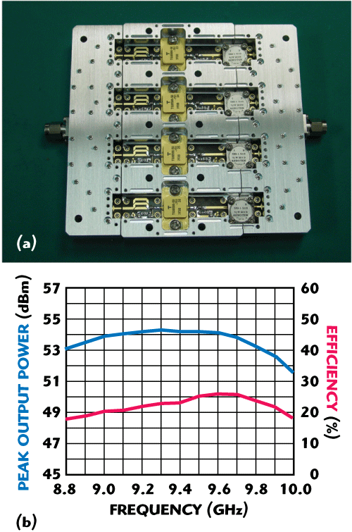
Figure 14 X-band 250 W GaN high power amplifier: (a) photograph and (b) RF performance.

Figure 15 Weather radar with GaN SSPA transmitter.
Conclusion
GaN HEMTs are the front-runners for the next-generation of high power devices, and developers foresee applications for these devices expanding from their initial use with pulse-mode operation for radar. Toshiba estimates that GaN devices with power output two to three times that of GaAs devices, above C-band, can be achieved by developing GaN technology to its full potential. The realization of such devices will accelerate the trend of replacing electronic tubes with SSPA in the amplifier market for terrestrial communications base stations, satellite communications earth station and radar use at C- to K-band (4 to 26 GHz) frequencies.
NOTE: Pentium is the registered trademark and the brand name of Intel Corp. and its subsidiaries in the US and other countries.
References
- E. Mitani, et al, “An 800 W AlGaN/GaN HEMT for S-band High-power Application,” 2009 CS Mantech Conference Digest, p. 213.
- K. Matsushita, et al, “C-band 150 W-class GaN Power HEMT,” Toshiba Review, Vol. 60, No. 12, 2005, p. 32.
- K. Yamanaka, et al, “C-band GaN HEMT Power Amplifier with 220 W Output Power,” 2006 IEICE General Conference Digest, C-2-24.
- 2006 Toshiba Press Release, http://microwave.toshiba.co.jp/snis/ovs/des/micro/technical/tech20061113.htm.
- K. Takagi, et al, “X-band 50 W-class GaN Power HEMT,” Toshiba Review, Vol. 62, No. 4, 2009, p. 42.
- 2009 Toshiba Press Release, http://microwave.toshiba.co.jp/snis/ovs/des/micro/technical/tech20091009.htm.
- K. Matsushita, et al, “Ku-band AlGaN/GaN HEMT over 65 W,” 2009 ISCS Conference Digest, p. 159.
- Y. Murase, et al, “CW 20 W AlGaN/GaN FET Power Amplifier for Quasi-millimeter-wave Applications,” 2009 CSICS.
- 2009 Fujitsu Press Release, http://pr.fujitsu.com/jp/news/2009/06/22.html.
- K. Matsushita, et al, “Reliability Study of AlGaN/GaN HEMTs Device,” 2009 CS Mantech Conference Digest, p. 87.
- K. Matsushita, et al, “AlGaN/GaN HEMTs Device,” 2005 CS Mantech Conference Digest, Paper 4.2.
- E. Mitani, et al, “A kW-class AlGaN/GaN HEMT Pallet Amplifier for S-band High Power Application,” Proceedings of the 2nd EuMIC Conference, p. 176.
- K. Kanto, et al, “An X-band 250 W Solid-state Power Amplifier Using GaN Power HEMTs,” 2008 IEEE RWS Conference Digest, p. 77.
- 2009 Toshiba Press Release, http://www.toshiba.co.jp/about/press/2009_11/pr_j2801.htm.
 Homayoun Ghani received his BS and MS degrees in chemical engineering from Tehran Polytechnic and his MS degree in electrical engineering from the University of California at Los Angeles. He joined TAEC in 2002, and has held various marketing and engineering management positions during that time, up to his current position. He is now manager of business development within the Discrete Business Unit of Toshiba America Electronic Components Inc., with marketing and engineering responsibilities for TAEC’s North American microwave, RF, logic and small-signal devices.