
For microwave systems that operate below 5 GHz, conventional circuit board materials are readily available with low cost and good performance. However, as systems migrate to higher frequencies, and as the demand for improved integration schemes increases, microwave and millimeter-wave designers look for the next generation of materials with improved versatility. Since its introduction to the microwave world about a decade ago, liquid crystal polymer (LCP) has become very attractive as a substrate and packaging material due to its unique electrical and mechanical characteristics.
One of LCP’s most attractive properties is its flexibility, which enables the emergence of conformal microwave circuits. The number of innovations that become possible using conformal electronics are endless. Sensors and wireless communication devices can be fabricated on LCP and integrated into fabric for use in military uniforms or personal health monitoring systems. Large antenna arrays can be assembled on LCP, rolled into a cylindrical shape, packed into a rocket payload, launched into space, and unrolled for a less costly deployment method since size and weight are minimized. A similar rolling and unrolling technique could be used by the military to quickly and covertly deploy an antenna array on the battlefield. The versatility of using LCP along with some of the advantages, limitations and challenges are discussed in this article. Several examples of state-of-the-art components and systems that are using LCP as a substrate or packaging material are presented.
It is widely accepted that as a technology matures, it typically shrinks in size, reduces in cost and offers improved performance. Often, these new technologies become a building block for product spin-offs. For example, a device that operates at S-band may be scaled to work at X-band. An emphasis is continually being placed on making devices that are versatile, scalable, reconfigurable, reliable and low cost. What makes this a challenge is the ability to choose microwave materials that are suitable for a broad spectrum of applications. The limiting factor at the module or system level is often the packaging. Improving the insertion loss of a device from 0.5 to 0.1 dB does not matter as much if the packaging losses are well over a dB.
In modern systems, an increased emphasis is being placed on 3D integration. The footprint size of a device can be greatly reduced by moving some of the components to a different vertical layer. These layers are connected with either metalized vias or capacitive coupling. Conventional materials, like low temperature co-fired ceramic (LTCC), can be used to make multilayer systems, but the high temperature firing (up to 900°C) makes it impossible to embed devices sensitive to high temperature.
An increased emphasis is also being placed on conformal and flexible electronics. The ability to wrap electronics around curved or angled surfaces can add new capabilities to modern systems. Laminating a receiver circuit flush against the nose cone of an aircraft, for example, may improve performance. Weaving a flexible circuit into a soldier’s uniform may create a comfortable and convenient way to carry communication devices.
For microwave systems that operate below 5 GHz, conventional circuit board materials are readily available with low loss and low cost. Materials like Duroid and FR4 have been in use for decades for everything from high school breadboard experiments to deep space satellites. As the frequency increases, however, the number of options drops quickly. Ceramic materials, like alumina and LTCC, start to become more attractive, but these materials have drawbacks of their own, including higher cost and dimensional instability during firing (a step necessary for multilayer systems).
Liquid crystal polymer (LCP) is a potential solution to all of the mentioned issues and shortcomings of conventional microwave materials. LCP is an organic material that offers low loss and dielectric stability from DC to 110 GHz,1 making it applicable to almost every consumer and military frequency band. With a permittivity of approximately 3, LCP is particularly appealing for antenna systems since the material naturally prohibits the excitation of surface waves. LCP can be made with a low melting temperature, which gives it a key advantage over other packaging materials. As system-on-package (SOP) approaches gain in popularity, LCP can provide a useful medium for multilayer and embedded designs.
Many current and next-generation microwave systems could benefit from using this unique material. In this article, the advantages and disadvantages of using LCP in modern electronics are discussed. Several emerging technologies that are taking advantage of LCP will be presented.
What is LCP?
LCP is a thermoplastic polymer made of aligned molecule chains with crystal-like spatial regularity. If heated to the liquid crystal state, rigid segments of the molecules align next to one another in the direction of shear flow. This structure persists even after cooling below the melting point. The uniform makeup of the material gives it unique electrical properties as well as strong mechanical and chemical properties.
LCP has been used for decades as a material for making sails, high strength rope and nets. In the 1980s, researchers started to make LCP in thin-film form. The first thin films made were brittle, non-uniform and would tear easily. By the 1990s, enough improvements had been made so that the material was suitable for high frequency applications.
One unique feature of LCP is that it can be made to melt at 290° or 315°C. The lower melting temperature material is called “bondply” and the other is called “core.” In all other electrical and mechanical aspects, the two materials are identical. To make a multilayer device with LCP, a layer of bondply is sandwiched between two core layers. The stack is compressed and heated to a temperature between 290° and 315°C. The bondply melts and chemically bonds to the core layers. Once bonded, the layers cannot be separated. Using this method, it is possible to bond together dozens of layers of LCP. An example of a multilayer stack-up (not to scale) is shown in Figure 1. Cavities are formed by cutting holes in the bondply before bonding and metal vias are used to connect the two layers.

It is important to consider that LCP is a polymer. It will never be as hermetic as ceramic and it will never be as thermally rugged as silicon. LCP is not intended to completely replace any conventional material, like FR4, Duroid, LTCC or alumina but, for many applications, LCP offers a distinct advantage. When the operating frequency exceeds X-band, many conventional materials become too lossy to use. LCP does not have this limitation. If the application can benefit by flexible or conformal electronics, LCP is an ideal option. When the footprint size must be minimized and a multilayer approach will be implemented, LCP becomes very attractive as a combination substrate and packaging material.
LCP Benefits
LCP combines the best qualities from almost every popular microwave material used today. Its electrical performance is comparable to that of polytetrafluoroethylene (PTFE), but it is as easy to fabricate as Duroid. Its multilayer capability rivals that of LTCC, but it can remain as flexible as paper. It can be as thin as 1 mil or extruded into any size and shape. It can be used as a substrate, a superstrate and a packaging material, but its cost is not much more than that of FR4. Several key benefits for using LCP are listed below:
• Wide frequency range: It has been shown that LCP offers low-loss (loss tangent less than 0.004) and dielectric stability from DC to 110 GHz.1 This wide frequency range makes LCP suitable for practically every application.
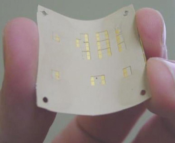
• Conformal: In thin-film form, LCP is as flexible as paper, as shown in Figure 2, where passive microwave devices and MEMS switches are embedded in the package. Only the coplanar waveguide probe pads are visible. It can be conformed into any shape and it can be laminated onto almost any surface. Extrusion and molding are also possible with this material.
• Low permittivity: LCP has a permittivity of approximately 3, which is electrically advantageous for packaging. The presence of a low-permittivity superstrate requires little or no additional design consideration. Packaging with a high permittivity material, like silicon, changes the impedance significantly and this must be taken into account.2
• Light weight: With a density of 1.4 g/cm3, LCP is 40 percent lighter than silicon, 65 percent lighter than alumina and almost 30 percent lighter than FR4. Air and space-borne applications greatly prefer light-weight materials.
• Biocompatible: LCP has been proven for safe use inside the human body (that is, it is non-toxic).
• Radiation resistant: LCP resists the harmful effects of radiation. This is advantageous for space-borne applications.
• Thickness variety: LCP can be made as thin as 1 mil or as thick as desired. This is ideal for antenna applications where the substrate thickness is determined by the tradeoff between wide bandwidth and low profile.3
• Low melting temperature: LCP bondply melts at approximately 290°C. Multilayer technologies are possible with embedded structures as long as the device can withstand short exposures at the melting point.3
• High dielectric strength: LCP has a dielectric strength of approximately 550 V/mil, making it suitable for high voltage and high power devices.
• Easy to process: LCP can be processed like any other material in a clean room. It is easy to laser cut or plasma process. It can also be drilled and machined.
• Low cost: As the technology matures, the cost of manufacturing LCP will continue to decrease. Currently, the price of LCP is comparable to that of other organic boards, like Duroid.
• Customized CTE: The coefficient of thermal expansion (CTE) of LCP can be tuned by changing the chemical formula. Values ranging from 3 to 30 ppm/°C are possible, but the standard CTE is 17 ppm/°C to match that of copper.
• Low moisture absorbing: LCP absorbs and retains only 0.02 to 0.04 percent of moisture by weight. The permittivity of water can be as high as 90 (depending on temperature and frequency) which, when absorbed, can have a profound effect on the substrate permittivity. By not absorbing moisture, LCP maintains a constant permittivity even in humid environments.3
• Chemical resistance: LCP is able to withstand prolonged exposures to harsh chemicals, even under high temperatures. This includes solvents, metal etchants, oxide etchants, strong acids and bases. Durations of constant exposure for over a month have been tested with a negligible change to the mechanical and electrical properties.
One area of microwave engineering that can greatly benefit from the advantages of LCP is antennas. The permittivity is high enough to keep the antenna size small, but low enough to minimize surface wave excitation (surface waves cause radiation pattern distortion, reduced efficiency and other negative effects). Thin LCP can be used for low-profile antennas and thick LCP can be used for antennas requiring higher bandwidth. The Sierpinski antenna shown in Figure 3 was made on 100 μm thick LCP.4 Micro-electro-mechanical (MEMS) switches were integrated to make the antenna frequency reconfigurable.
Since the material is flexible, conformal antennas on LCP are possible. For example, a large antenna array could be laminated onto the side of an aircraft fuselage or the nose cone of a rocket. Since the material does not absorb moisture and can withstand chemical exposure, it is well-suited for outdoor deployment. Antennas are scalable by frequency and a material that operates across a wide frequency spectrum is usually desired. A unique antenna design could be scaled to work for L-band communications or W-band collision avoidance using the same material for both applications. This can provide considerable cost savings.
The benefits for using LCP are not restricted to only multilayer and conformal systems. It can also be used as a low-loss substrate for rigid circuits. The cost of LCP is currently not low enough to make it competitive against FR4 for rigid circuits operating at less than 10 GHz. However, for X-band and higher, LCP would excel as a rigid substrate material. There are several fabrication companies that currently offer LCP as a circuit board material, including Modular Component National (www.modularcomp.com) and Dynaco Corp. (www.dynacocorp.com).
LCP Limitations
Even though LCP has many ideal properties, it does have some limitations. For example, it is an insulator so it cannot be used as the bulk material of a transistor (although it can be used as a carrier for bare die and packaged transistors). It is a polymer, so it cannot be used to make a hermetic package. Some of LCP’s current limitations and misconceptions are listed below:
• “Near-hermetic”: Since LCP is a polymer, it cannot be truly hermetic. Although the extent of LCP’s hermeticity is still under debate, the general consensus is that LCP performs well in gross-leak testing, but poorly in fine-leak testing. Micro-cracks in the LCP packages are effective at repelling liquid, but not moisture (such as vapor). The material itself absorbs very little moisture, as previously discussed. For this reason, LCP is commonly classified as “near-hermetic.”5
• New material: LCP is often considered a new material and is therefore too experimental to be used in a developing system. Actually, LCP has been used in its current form for almost a decade with consistent performance.
• Strong bases: LCP is chemically resistant and has demonstrated no deterioration with prolonged exposures to strong acids. However, strong bases, especially when heated, will dissolve LCP over time. For example, photo resist remover with a pH of 12 will dissolve a piece of LCP in less than 24 hours if heated to 60°C. This sensitivity to strong bases is true of all organic materials.
• Poor thermal conductor: Since LCP is a polymer, it does not conduct heat well. Any heat that is generated inside of an LCP package will not dissipate quickly. However, LCP does provide a thermal barrier to any heat sources outside of the LCP package. Depending on the application, poor thermal conductivity can be beneficial or problematic.6
• Surface roughness: LCP has a natural surface roughness of a couple of microns. By comparison, a polished silicon wafer may have a surface roughness of a couple of nanometers. For applications that require a polished surface, the LCP must be mechanically polished before using. This is not a difficult process and can be performed at production scale.7
Current LCP Innovations
LCP certainly has the potential to provide never before seen consumer and military innovations. Conformal electronics are rarely heard of because flexible materials are not readily available. A few decades ago, a low-cost, flexible, low-loss material that could operate to 110 GHz was unheard of and inconceivable. Today, LCP can do all of these things and more. Microwave engineers have been using LCP for nearly a decade and several exciting new technologies have emerged from this effort. The Georgia Electronic Design Center (GEDC) at Georgia Tech is one of the key research facilities for LCP technologies. Since LCP is very advantageous for antenna systems, most of the research that has been performed to date is focused on novel antenna designs and systems. Several examples of recent LCP innovations are presented below.
RFID
A radio frequency identification (RFID) tag or transponder is a device capable of storing and wirelessly transmitting a packet of information. These devices can be integrated into products, animals and even people for providing fast and secure identification. Many department stores are currently using RFIDs to monitor their products. A toll pass transponder that commuters can use to pay their fee without stopping is another example of an RFID.
LCP is particularly attractive for RFID antennas because it lends itself well to conductive printing techniques. In this process, LCP can be fed into an inkjet printer similarly to a piece of paper and the antenna pattern can be printed on using a conductive ink. This fabrication method has the potential of being fast and super low-cost, which are key elements to a successful RFID. The ultimate goal is to place an RFID tag on every consumer product for easy tracking.

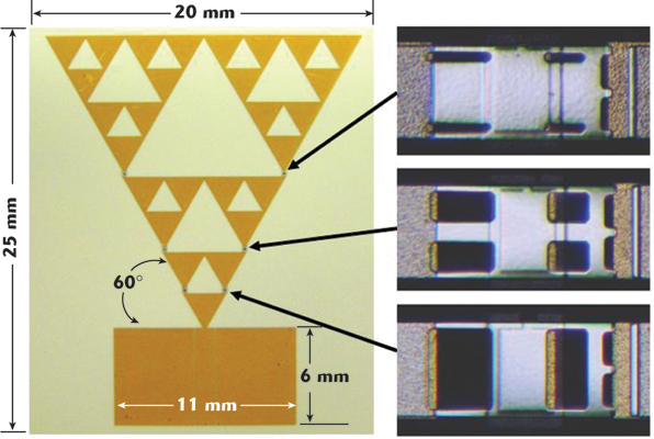
The “Printed Electronics Laboratory” at the South Dakota School of Mines and Technology is one of the leading research facilities for conductive printing on LCP. The ultra-wideband (UWB) antenna shown in Figure 4 was designed by Dimitris Anagnostou and fabricated by Ahmad A. Gheethan using an M3D (Maskless Mesoscale Materials Deposition) machine.8 On a piece of unpolished LCP, a printing accuracy of ±20 μm is possible with this technique.
Inflatable Arrays
Organizations like NASA have been interested in using LCP as a satellite antenna material since it was first introduced. Deploying a large satellite in space is challenging because it must be able to fit inside a rocket or Shuttle payload. Ideally, a large antenna array could be rolled up like a round bale of hay, loaded into a rocket, blasted into space, deployed into orbit, and unrolled, as demonstrated in Figure 5.7 This method minimizes the size of the rocket needed to launch the payload, which drastically reduces the cost of satellite deployment.

The military has also been interested in inflatable arrays for some time. A large array can be packed tightly for easy mobility and quickly deployed on the battlefield as needed. When not in use, the inflated array can be deflated and packed away. Both of these processes are much more covert, because they allow for easy mobility and a negligible radar cross section when not in use.
MEMS Switch Substrate and Packaging
The ability to make MEMS switches directly onto a polymer material offers an opportunity to greatly decrease the cost of a MEMS device. The high cost of MEMS is due partly to the expensive metal and ceramic packaging. MEMS are incredibly sensitive to heat and moisture, so careful packaging is essential. Aside from cost issues, ceramic packaging can be lossy and bulky as well.
MEMS can be fabricated on LCP after polishing the surface to a mirror finish. At that point, the surface roughness is no longer an issue for reliable operation. MEMS switches on LCP have demonstrated hundreds of millions of cycles and testing is still in progress.7
MEMS can be packaged in LCP, but unfortunately most MEMS devices cannot survive the 290°C bonding temperature. Therefore, other bonding methods have been explored. Some examples of localized bonding techniques that have been investigated include metal rings,6 infrared lasers and ultrasound. The four-bit switched-line phase shifter shown in Figure 6 was packaged in LCP using epoxy. A cavity was formed in the bondply to protect the MEMS tree-junctions.7 This MEMS phase shifter is one of the passive devices packaged in the flexible circuit shown previously.

Communication Module
For a long time, the Holy Grail of 3D integration was to combine active, passive and electromechanical devices onto one multilayer package. Such a technology would demonstrate that system-on-package (SOP) design strategies were possible.
In the spring of 2007, researchers at the Georgia Institute of Technology created a fully functional, multilayer receiver module on LCP. A 2 x 2 patch antenna array was integrated with MEMS reconfigurable phase shifters to create a beam steering array. A low-noise amplifier (LNA) was used to amplify the received signal. The LNA could have been replaced with a power amplifier to create a transmit module as well. The operating frequency of the device was 14 GHz for satellite communication applications.9
The researchers implemented the module using a single layer and a multilayer approach. By moving the LNA to a different vertical layer, they were able to reduce the size of the module by 25 percent. The single layer implementation is shown in Figure 7 and the flexibility is demonstrated.7

Conclusion
LCP was introduced to the microwave industry almost a decade ago and since then many companies, universities and national laboratories have used the material in their designs. For applications requiring flexible or conformal electronics, LCP is the forerunner in microwave materials. Even as a rigid board material, LCP offers low-loss performance through W-band, dielectric stability and low cost.
LCP is also an excellent packaging material. With a low melting temperature bondply available, making a multilayer device is a straight-forward process. Since the permittivity is low, very few design considerations need to be given to the packaging effects.
To date, most of the innovations being developed with LCP are antennas. LCP is well suited for antenna applications due to its dielectric stability, wide frequency range, low permittivity and resilience to harsh environments.
Researchers are already planning future microwave systems that are more compact, lighter-weight and better performing. To do this, versatile materials are desired that can satisfy a variety of electrical and mechanical needs. LCP is ready to fulfill the requirements of current and next generation systems.
Acknowledgments
The author would like to thank John Papapolymerou and Manos Tentzeris at Georgia Tech for their research efforts that have inspired this article. He would also like to thank George Ponchak at NASA Glenn for supporting the LCP antenna deployment and communication module programs. Lastly, the Rogers Corp. is thanked for providing the LCP material and supporting much of this research.
References
1. D. Thompson, O. Tantot, H. Jallageas, G. Ponchak, M. Tentzeris and J. Papapolymerou, “Characterization of Liquid Crystal Polymer (LCP) Material and Transmission Lines on LCP Substrates from 30 to 110 GHz,” IEEE Transactions on Microwave Theory and Techniques, Vol. 52, No. 4, April 2004, pp. 1343–1352.
2. D. Thompson, N. Kingsley, G. Wang, J. Papapolymerou and M. Tentzeris, “RF Characteristics of Thin-film Liquid Crystal Polymer (LCP) Packages for RF MEMS and MMIC Integration,” 2005 IEEE MTT-S International Microwave Symposium Digest.
3. Rogers Corp., “RO3000 Series High Frequency Circuit Materials,” http://www.rogerscorporation.com/mwu/pdf/3000data.pdf, May 2005.
4. N. Kingsley, D.E. Anagnostou and J. Papapolymerou, “RF MEMS Sequentially-reconfigurable Sierpinski Antenna on a Flexible Organic Substrate with Novel DC-biasing Technique,” IEEE Journal of Microelectromechanical Systems, Vol. 16, No. 5, October 2007, pp. 1185–1192.
5. N. Kingsley, S. Bhattacharya and J. Papapolymerou, “Moisture Lifetime Testing of RF MEMS Switches Packaged in Liquid Crystal Polymer,” IEEE Transactions on Components and Packaging Technologies, to be published in April/May 2008.
6. M.A. Morton, N. Kingsley and J. Papapolymerou, “Low Cost Method for Localized Packaging of Temperature Sensitive Capacitive RF MEMS Switches in Liquid Crystal Polymer,” 2007 IEEE MTT-S International Microwave Symposium Digest.
7. N. Kingsley, “Development of Miniature, Multilayer, Integrated, Reconfigurable RF MEMS Communication Module on Liquid Crystal Polymer (LCP) Substrate,” PhD Dissertation, Georgia Institute of Technology, May 2007.
8. Image used with permission by Dimitris Anagnostou, Electrical and Computer Engineering Department, South Dakota School of Mines & Technology.
9. N. Kingsley, G. Ponchak and J. Papapolymerou, “Reconfigurable RF MEMS Phased Array Antenna Integrated Within a Liquid Crystal Polymer (LCP) System-on-Package,” IEEE Transactions on Antennas and Propagation, Vol. 56, No. 1, January 2008, pp. 108–118.

Nickolas Kingsley received his PhD degree from the Georgia Institute of Technology in May 2007. During his PhD program, he focused on novel technologies using liquid crystal polymer (LCP) substrate. He joined Auriga Measurement Systems in June 2007 as a principal engineer in the measurement, modeling and design group. His research interests include the design, miniaturization, fabrication, packaging and testing of RF MEMS multilayer front ends.