The automatic gain control (AGC) circuit is a critical building block in modern wireless transceivers. It is used in both the transmitter (TX) and receiver (RX). In the TX, the AGC is used to regulate the output power level. For example, a well-known issue in a CDMA system is the problem of simultaneously receiving two signals of different strength. If two users transmit to the base station (BS) at the same time, the received power from the close user will be much higher and will jam the signal from the far away user if the power level difference is large. It is desirable to use an AGC to control each TX’s output power so that the power received from all users is equal. In the RX, the received signal can vary drastically in a mobile environment. At the same time, the analog-to-digital converter (ADC) requires a fixed input level. An AGC circuitry can be used to stabilize the received power level at the ADC’s input.
Original equipment manufacturers (OEM) demand highly integrated transceiver integrated circuits (IC) from RFIC vendors. CMOS technology has been the technology of choice because of its low cost and higher integration features. This article focuses on the AGC implementations in CMOS technology. AGC circuitry has been well studied and researched. This article presents seven widely used topologies for the AGC, including variable transconductance, variable degenerated feedback, variable biasing at the gate, variable biasing at the source, variable supply, variable feedback and variable T network. Each topology is discussed in detail.
The control voltage is an important topic. It is highly desirable to have a gain control voltage that behaves exponentially with the input voltage. The purpose is to achieve a wide dynamic range or a linear-in-dB performance. The gain control voltage has to be well regulated against temperature and process variations. The gain control circuitry is an art by itself. It deserves a detailed discussion in a separate article. Here, the control voltage is assumed.
Variable Transconductance AGC
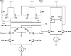
The variable transconductance AGC circuit is shown in Figure 1. Its fundamental theory is based on a FET’s gain variation as the FET changes from a saturation mode to a triode mode. In the saturation region, the current-voltage (I-V) curve has the steepest slope, thus the highest gain. As the mode changes, the slope begins to flatten out. M1 and M2 are the gain blocks. Their operating mode is controlled by the gate voltage of M3 and M4. The drain voltage of M1 and M2 is equal to Vcont – Vgs (M3 and M4). Vgs1 – Vt + Vgs3 is the borderline value for Vcont. Above it, M1 and M2 are in the saturation region (high gain). Below it, M1 and M2 are in the triode region (low gain). As Vcont transitions from a high to a low voltage, the gain will follow accordingly. The load in this circuit is of the current source type. M7 and M10 are the primary load. M8 and M9 are the bleeding elements used in the common mode feedback (CMFB). The reason for using a CMFB circuit is because of the current source type load. The drain voltages at M3 and M4 are not well defined. The mismatch between the PMOS (M7, M10) and the NMOS current source (I1) will pull M7 and M10 into a triode region from the desired saturation region. M5 and M6 are the common mode sensing resistors implemented with the FETs. This voltage is compared to a reference voltage. The error voltage is fed back to control the bias current in the bleeding current source (M8 and M9). The comparator is implemented with M11 to M14. This variable conductance AGC works well, up to a low gigahertz range.1
Variable Degenerated Feedback AGC
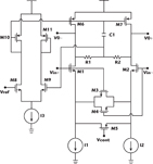
An AGC with a variable degenerated feedback is shown in Figure 2. Its fundamental principle is to vary the degenerated feedback resistor in a differential amplifier. The gain of the differential amplifier is proportional to the ratio of the load resistance to the feedback resistor. As the degenerated feedback resistor’s value is varied, AGC is accomplished. M1 and M2 are the differential amplifier pair. M5 is the degenerated variable feedback resistor implemented with a FET in the triode region. M3 and M4 are the fixed degenerated resistance to improve the linearity of the gain block. Again, the CMFB with FETs from M8 to M11 are used in this circuit to keep the current source load M6 and M7 in the saturation region. There are two differences in this CMFB implementation. First, the true sensing resistors R1 and R2 are used. Second, the feedback voltage directly controls M6 and M7 without the bleeding elements. This implementation works better at low frequencies2 because the variable resistance M5 is not well controlled at a high frequency due to the parasitic capacitance.
Variable Gate Biasing AGC

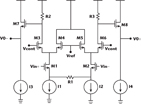
The AGC with a variable biasing at the gate is shown in Figure 3. This topology works well at gigahertz frequencies and is widely used. Its fundamental principle is to vary the gain by controlling the bias current. The gain control voltage is compared to a reference voltage. If the gain control voltage is higher, it will supply more current to the gain element, thus the amplifier will have more gain. M1 and M2 are the basic differential amplifiers. M3 to M6 form the comparing stages. They provide gain as well, when their bias current is increased. In that case, the gain stage can be considered as a differential cascode circuit. M7 and M8 are the output buffers to lower the output impedance. The variable bias current at the gate is well suited for high frequency operation because of its simplicity.
Variable Source Biasing AGC
A variable bias can be done either at the gate or the source. The variable bias at the source is shown in Figure 4. Its principle is the same as for the variable gate biasing, only this time the gain control is done by varying bias current at the source. The circuit shown is a much-simplified version. The CMFB circuit is omitted, since it is similar to the ones shown previously. The AGC performance is similar to the one shown for the variable gate biasing circuit.
Variable Supply AGC
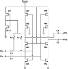
A variable supply AGC, shown in Figure 5, is easy to understand and easy to implement. It has been reported in the literature.4 The basic gain element is a CMOS inverter biased at one half of Vdd. When a CMOS inverter is biased at Vdd/2, its I-V curve is at the steepest point, thus it has a large gain. By varying the supply, the slope will change. Hence, a variable gain can be accomplished. M1 and M7 and M2 and M8 are two pairs of inverters, one for each of the differential input signals. M3 to M6 are the switches to reduce leakage between the input and output of the inverter amplifier. They are always on. The leakage will reduce the AGC range if it is not dealt with. M9 and M10 are essentially a resistor divider to obtain one half of Vcc.
Variable Feedback AGC
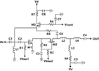
A variable feedback AGC is described next. Gain control using feedback is well known. Such a design is shown in Figure 6. The amplifier’s gain comes from a common source stage M1 and a common gate stage M2. C1, C2 and L1 are the input-matching elements. L1 doubles as the DC return for M3. L2 and L4 are the output-matching network. L3 is a radio frequency choke. The variable feedback path consists of M3, R5 and C6. C6 is selected to be a short circuit at the frequency of the interest. Excellent RF VGA performance has been reported.5
Variable T Network
In an AGC circuit the gain control block and the gain block are sometimes separated to have a more modular design. In those instances, a gain control block can be a voltage variable attenuator (VVA). The VVA has been used for a long time in the microwave industry. With the continuous improvement in CMOS technology, a VVA implemented in CMOS technology has gained popularity.6,7 The basic principle of a VVA is a variable resistive pad. A fixed attenuation pad is typically implemented with three resistors in a T or a Pi network. For example, a T network with two series 26 Ω resistors and a shunt 35 Ω resistor will give 10 dB attenuation. By varying the shunt and series resistances complementarily, the VVA operation can be done easily. A two-stage T variable pad is used in Figure 7. M2 is used to further improve the attenuation range. With a good CMOS process, the RF portion can be implemented fairly easily. The difficult part is to generate a precise control voltage for the series and the shunt FETs. The variable T or PI network VVA is well suited for broadband and high frequency operation.

Conclusion
There are many topologies at the disposal of CMOS transceiver IC designers. Seven different designs based on different principles are presented and discussed. Each one has its pros and cons. For example, a variable T network is a very good topology for high frequency operation, but offers no gain. A variable transconductance AGC is a high performance circuit, but requires a CMFB circuit, increasing the complexity and limiting the upper operating frequency. It is beneficial for the IC designer to realize the strengths and weaknesses of each topology. A comparison between the different approaches is given in Table 1. An AGC topology needs to be carefully examined and selected for the specific application at hand.
References

1. H.D. Lee, K.A. Lee and S.C. Hong, “A Wideband CMOS Variable Gain Amplifier with an Exponential Gain Control,” IEEE Transactions on Microwave Theory and Techniques, Vol. 55, No. 6, Part 2, June 2007, pp. 1363–1373.
2. Y. Zheng, et al., “A CMOS dB-linear VGA with Pre-distortion Compensation for Wireless Communications Applications,” Proceedings of the 2004 IEEE International Symposium on Circuits and Systems.
3. W. Hu, et al., “Design of a 1.8 V High Frequency CMOS Variable Gain Amplifier with a Novel dB-linear Gain Structure,” 47th IEEE International Midwest Symposium on Circuits and Systems.
4. A. Ismail and A.A. Abidi, “A 3.1 to 8.2 GHz Zero-IF Receiver and Direct Frequency Synthesizer in 0.18 μm SiGe BiCMOS for Mode-2 MB-OFDM UWB Communication,” IEEE Journal of Solid-State Circuits, Vol. 40, No. 12, December 2005, pp. 2573–2582.
5. M. Ito, et al., “Variable Gain Amplifier in Polar Loop Modulation Transmitter for EDGE,” 2005 IEEE ESSCIRC, 31st European Solid-State Circuit Conference.
6. K. Nishikawa and T. Tokumitsu, “A MMIC Low Distortion Variable Gain Amplifier Using Active Feedback,” IEEE Transactions on Microwave Theory and Techniques, Vol. 43, No. 12, Part 2, December 1995, pp. 2812–2816.
7. H. Dogan, et al., “A DC-10 GHz Linear-in-dB Attenuator in 0.13 μm CMOS Technology,” 2004 IEEE Custom Integrated Circuits Conference.
8. H. Dogan, et al., “A DC–2.5 GHz Wide Dynamic Range Attenuator in 0.13 μm CMOS Technology,” 2005 IEEE Symposium on VLSI Circuits Digest of Technical Papers.
9. S. Tadjpour, et al., “A CMOS Variable Gain Amplifier for a Wideband Wireless Receiver,” 1998 IEEE Symposium on VLSI Circuits Digest of Technical Papers.
Louis Fan Fei received his BSEE and MSEE degrees from Georgia Tech in 1996 and 1998, respectively. He worked on microwave instrument circuits for HP/Agilent in Colorado Springs, CO, in the summer of 1997 and on WLAN and wireless local loop circuits at Lucent/Agere Systems from 1998 to 2003. He is now an RF engineer at Garmin International, where he designs GPS receivers.
