How would you like to design circuits with perfectly shielded, low-loss, purely TEM broadband transmission lines, which could be stacked next to and on top of each other with no coupling? The lines can be tens of centimeters long, cross at multiple levels and at any angle, and holes could be left to plug in actives or other surface-mount components. Impossible? A radically new way to design and fabricate microwave and millimeter-wave circuits recently grew from an idea to reality: PolyStrata™ microfabrication technology offers the possibility of producing miniature, dense and very complex three-dimensional (3D) metallic-dielectric components with an unprecedented ability to go directly from 3D CAD drawings to identical intricate 3D miniature circuit components.1 As a result, one can now design dense multi-layer meshes of micro-coaxial cables that do not couple to each other and operate with low loss well into the millimeter-wave region.
Figure 1 shows a photograph of a portion of a phased array with reactively-loaded patch antennas and a feed network implemented in air-filled micro-coaxial lines made of copper. This is the first wafer-scale integrated coaxial millimeter-wave phased array that includes a Butler matrix coaxial beamformer, air-patch antennas, and MMIC switches and amplifiers. The entire phased array is 15 x 2 cm in area.
The PolyStrata microfabrication process is the first manufacturing technology that can deposit a dozen or more precision patterned layers of both metals and polymers on a flat sheet, and then release them to allow gaps and mechanical flexibility, resulting in sophisticated miniature devices with features ranging from a few microns to several centimeters. Dozens to thousands of devices can be fabricated on a single substrate. With this technology, it is possible to dramatically reduce the size of coaxial lines, actuators, valves, engines, motors, pumps, sensors and other electromechanical products that would otherwise be impractical or impossible to produce with other manufacturing approaches. Great freedom in realizing structural designs is possible with finished parts matching their CAD designs with micron level accuracy. The added degrees of freedom allow the designer to work with completely new components, as well as to fabricate components that are difficult or impossible to machine or fabricate otherwise, such as high-frequency waveguides and antennas.
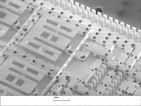
Commercialization of PolyStrata components at Rohm and Haas is currently focused on one market segment—microwave electronics. The technology and patented process for “air-core recta-coax” is the key to miniaturized 3D microwave devices for new high-quality circuits that can be either monolithically fabricated as a free-standing module or can be released from the substrate to create surface-mountable components for other substrates. Its greatest value lies in its delivery of superior performance, integration, size reduction and cost reduction for products in the 10 to 200 GHz range. These frequencies are of increasing use and interest for the evolving needs in military communications, radar and sensing systems, and are of rapidly growing interest for civilian applications such as automotive radar, satellite communications, cellular back-haul, point-to-point data links and terahertz imaging.
Currently much of the development funding for PolyStrata technology comes from the Department of Defense (DoD) through the Defense Advanced Research Projects Agency (DARPA) under two major programs: 3D-MERFS (3D Micro-Electrical-RF-Systems), which is developing millimeter-wave phased arrays for satellite communications, and DMT (Disruptive Manufacturing Technologies), which is developing broadband GaN-PolyStrata hybrid microwave amplifiers. Both of these programs are being developed with defense contracting partner BAE Systems Inc. and in collaboration with electromagnetic and circuit design researchers at the University of Colorado at Boulder.
Fabrication techniques such as precision milling, EDM and silicon micromachining have achieved some success in making basic circuit structures. Meanwhile, the smaller size possible in transmission lines such as microstrip and coplanar waveguides used in MMICs and hybrid circuits have been relegated primarily to 2D or at best 2.5D planar structures with reduced performance at higher frequencies due to loss, dispersion and isolation. In contrast, the PolyStrata process is a fully 3D fabrication technique, which employs additive sequential-build micro-forming.
In the PolyStrata microfabrication process, metal and dielectric patterns are formed into a series of polymer molds and planarized multiple times, as illustrated in Figure 2 for the simple cross-section of a square air-filled coaxial line. Each layer can be from 10 μm to over 100 μm thick, for example, with high aspect ratios with a dozen or more layers that are fused together. At the end of the process, the polymer mold material is removed through release holes in the metal, leaving air in its place with free-standing metal and dielectric structures behind. The release holes are designed to introduce minimal radiation and ohmic loss and are electrically small for all frequencies of interest. In order to support freestanding structures such as the center conductor of the coaxial line, thin (5 to 25 μm) patterned low-loss dielectric strap holders are added in the process. The dielectric straps can also be designed to support thin-film microelectronic materials such as SiCr for integrated resistors. Currently, the bulk-electroformed metal is copper, which can be post processed with tarnish-protective electroless silver or nickel-gold coatings.
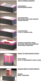
All the processes typically occur at temperatures below 150°C, allowing the possibility of building the structures directly on completed wafers of active devices. The finished components can stay on the substrate on which they are built, but can also be chemically released and flip-chip mounted or soldered onto any other substrate or on top of other PolyStrata devices.
The fundamental properties of PolyStrata air-filled micro-coaxial lines and the resulting advantages for microwave and mm-wave systems include:
• Ultra-low dispersion. As the size of a coaxial line is reduced, the frequency at which modes other than the TEM mode can propagate increases. The dielectric straps that hold the center conductor are a very small fraction of the volume of the coaxial line (< 1 percent), and have an extremely small effect on wave propagation along the coax. Although strictly speaking the mode is quasi-TEM because of the dielectric, for all practical purposes the mode can be considered as TEM up to very high frequencies. For example, for a 250 μm square-cross-section coaxial line, the TEM mode propagates alone up to > 450 GHz.2 The TEM mode locally has the same properties as a uniform plane wave, that is, the phase velocity, group velocity and impedance are not functions of frequency. Thus, very broadband components can be designed using this type of line as a building block. For example, a 20 to 50 GHz bandwidth Lange coupler is easily designed using PolyStrata technology.3 In addition, the process aspect ratios allow lines with characteristic impedances between 15 and 100 Ω to be fabricated in the same fabrication run.
• Very low loss per wavelength. Loss in guided wave components is due to metallic loss, which increases with frequency due to the skin effect and roughness, and dielectric loss due to the finite conductivity of the insulating material. It is fairly easy to show that even if the dielectric in a coaxial line is perfect, the lowest loss corresponds to the lowest relative permittivity, that is, to an air dielectric. The very first measurements of 250 μm wide lines fabricated with 5 copper layers showed a loss of 0.18 dB/cm around 26 GHz,2,4 while more recent results with added layers demonstrate as low as 0.07 dB/cm loss around 38 GHz.5
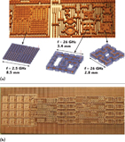
• Extremely high isolation. A coaxial cable is a shielded line, and although the PolyStrata process typically employs release holes in the outer conductor to dissolve out the lossy dielectrics used in processing, careful electromagnetic design of the hole position, number and size has resulted in very low radiation. Measured coupling between two lines that are fabricated with touching outer conductors is below –60 dB through 50 GHz.5 Independent testing by the Mayo Institute demonstrated measured cross talk at Ka-band (37 GHz) between lines on a 200 μm pitch to be less than –62 dB, which was the noise floor of the measurement system. The extremely high isolation between neighboring lines enables dense interconnects, components with drastically reduced size and 3D layouts that give an entire new degree of freedom in circuit design. Figure 3 illustrates the possibilities in size reduction of standard components using this technology over a range of frequencies. This type of new design enables extremely high-density circuits. For example, in the Butler matrix feed for a phased array, there were 1534 transmission line elements in an area of 5.65 cm2.
To illustrate some of the fundamental properties previously discussed, a simple comparison with standard technologies is shown in Figure 4. As can be seen, compared to microstrip or CPW on GaAs or alumina, Polystrata micro-coaxial lines have the best loss-isolation combination.
Most multi-layer transmission line media require a solid dielectric, such as in the case of LTCC and multi-layer fluoropolymer materials. Although these technologies provide high-density interconnects and have relatively low loss up to W-band,6 the PolyStrata approach has advantages in terms of lower loss, much lower dispersion and significantly reduced coupling for neighboring lines, thus allowing high density circuits. The micro-coax lines hold promise for applications at frequencies significantly above W-band. In addition, PolyStrata micro-coaxial lines have a much larger fraction of the volume that is metallic, allowing for improved heat management with a thermal conductivity of nearly 400 W/mK.

Initial efforts to microfabricate air-filled coaxial components were reported.7–9 These researchers examined air-filled coaxial transmission lines in addition to other high-quality air-filled millimeter-wave technologies. The micro-fabricated coaxial technology discussed in References 10 through 16 with a nickel-based N-layer process and periodic metal supports for the inner conductor has been used to demonstrate couplers, filters and resonators. Air-filled coaxial components produced by stacking laser micromachined layers in which the center conductor is suspended using short-circuiting stubs is investigated in Reference 17. PolyStrata technology has the unique advantage of producing multiple layers of coax, producing coax with a dielectrically isolated center conductor, incorporating embedded thin-film microelectronics on the embedded dielectrics, and producing all of this using scalable manufacturing processes. These accomplishments have been in part realized by engineering an application specific set of materials by Rohm and Haas especially for this process, including a new negative photoresist mold material that can dissolve without swelling.
A number of publications to date describe in detail the electrical properties of the air-filled copper micro-coaxial lines and passive components such as resonators, branch-line couplers and antennas, which were realized in the first implementations of PolyStrata technology over the past couple of years.1–5,18–22 Table 1 illustrates the design, fabrication and measured characteristics of several specific devices demonstrated in the first generation of PolyStrata components developed in the DARPA 3DMERFS program. The left-hand column shows the CAD models of a Ka-band branch-line hybrid,19 a cavity-backed antenna21 and a quasi-planar high-Q resonator.22 Starting from a zero-order circuit model, a specialized layout routine enables automatic creation of files corresponding directly to the complete geometry of the component, including release holes, dielectric straps and any interconnects. The resulting file can be directly imported for simulation in the Ansoft HFSS FEM tool. After optimization using full-wave electromagnetic analysis, the CAD files are used for PolyStrata fabrication at the Rohm and Haas fab in Blacksburg, VA. Photographs of fabricated devices corresponding directly to the CAD drawings in the first column are presented in the second column. Calibrated measurements using off- or on-wafer calibration standards are then performed and compared to predicted performance, as shown in the third column. Component specifications are collected from measured data on a number of components across a wafer.
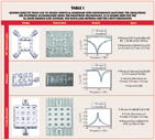
The performance of the first generation of PolyStrata components is excellent. For example:
• the hybrids have an amplitude and phase mis-balance of < 0.1 dB and two degrees over a five percent bandwidth centered at 35 GHz;
• the antennas have a five percent 2:1 VSWR bandwidth with 6.8 dBi predicted gain at 36 GHz;
• the miniaturized resonators have an unloaded Q factor over 830.22 In addition, for a given cavity height, normalized by frequency, the record high unloaded Q for a microfabricated cavity resonator has been demonstrated.20
Other components that have been designed and are either already fabricated and characterized or in the process of fabrication include:
• 1:2, 1:3, 1:4 divider/combiner networks in the frequency range from 2 to 110 GHz;
• micro-coaxial baluns and transformers that are broadband, e.g. 2 to 14 GHz;
• a variety of couplers from C- to W-bands: branch-line hybrids, rat-race hybrids and broadband Lange couplers; narrowband antennas, such as cavity-backed patches and coaxial co-linear arrays; filters and duplexers using both coupled cavity designs and transmission-line resonator designs up to Ku-band;
• monolithically integrated embedded resistors both in-line for low power applications and on-substrate for high-power applications;
• micro-coaxial lines with a range of impedances from 12 to 110 Ω;
• millimeter-wave (above W-band) rectangular dominant-mode waveguides and waveguide-coaxial adaptors;
• jumpers and cross-overs with extremely low coupling up to W-band that can be integrated or surface or flip-chip mounted;
• interconnects from microcoaxial lines to CPW probes, CPW on the substrate, CPW flip-chip pads on a different substrate, microstrip, as well as transitions to connectors and waveguides; and
• high-quality and current handling lumped inductors integrated in series or parallel with the microcoaxial line.
In addition, Rohm and Haas and AFRL have been jointly exploring millimeter-wave applications of PolyStrata under a cooperative research agreement (CRADA 07-291-SN-01). Under this agreement, the Air Force is investigating the benefits of PolyStrata for millimeter-wave components such as filters, voltage-controlled oscillators and wideband switch matrices. Successful testing of 40/50 GHz diplexers has recently been completed and the results will be submitted for publication soon.
Many of these and other building block components will be characterized, parametric models produced and a design library generated. This library can allow designers to import these elements into circuit simulators to realize their own microwave systems in the Polystrata technology.
The micro-coaxial environment combined with the PolyStrata technology allows improved components, but also allows the creation of new types of components, which can be integrated in different ways into hybrid monolithic integrated circuits (HMIC). Due to the lithographic nature of the fabrication, tolerances are on the order of a few microns across tens of centimeters of line length. This allows a complete toolbox of phase-controlled components to be transferred directly into the technology eliminating the parasitics, cost, and space associated with interconnects and device mounting tolerances when mounting discrete devices in traditional assemblies.
In order to obtain high-performance military and commercial EHF modules, there needs to be an attractive means to bring the best passive and active technologies together. Unfortunately, these have not converged to a single active semiconductor platform with the best technologies desired for amplifiers, digital circuits, mixed signal circuits, phase shifters, tuners and switches. Thus, heterogeneous hybrid active device integration is currently being developed through the monolithic creation of device “sockets” that allow both flip-chip and wire-bond integration. The sockets can be designed to handle devices from the transistor level (200 x 200 μm die) up to relatively large ICs and MMICs, and with a relatively high positional tolerance. Thus, traditional flip-chip mounting tools can be used while still minimizing parasitic reactances. Such sockets integrate both thin film solders, diffusion barriers and solder wick-stops to allow direct chip attach. Alternatively, active-side-up mounting and wedge bonds into such sockets is also possible when either metallurgy or on-chip parasitics make flip-chip difficult. Due to the PolyStrata backplane being composed primarily of metallic copper, thermal mounting pads and heat-routing solutions can be directly implemented allowing both rapid local spreading and transfer of heat to secondary heatsinks and thermal back-planes. Multi-die mounting challenges are being addressed by the use of transient liquid phase solder stacks, such as the Au-Sn system, that can be made to reflow only once for a limited time when heat is pulsed through the die to be mounted. CTE differences are addressed by building compliant structures directly into the socket. Solving the challenging work on active device integration for high thermal density components, specifically GaN, is ongoing through DARPA support of the Disruptive Manufacturing Technologies (DMT) program.
Where can PolyStrata micro-coaxial technology help? Commercial applications for the technology include miniature radar systems and components, satellite matrix switches, lossless baluns for phase matching of power amplifiers to their packages, high-Q inductor banks for filters, point-to-point EHF data link components, antenna diplexers, low-loss power combiners for solid-state microwave amplifiers and automotive radar systems. Rohm and Haas is actively seeking partners to develop the technology for these and other applications.
Military applications are numerous due to the extremely high performance characteristics of the demonstrated components and the dramatically improved size and isolation compared to existing technologies. The goal of the 3D-MERFS DARPA program is to produce assemblies of PolyStrata panels for phased arrays for on-the-move multi-point communications including SATCOM. This will enable high bandwidth real time data communications between command vehicles, air vehicles and global command stations using satellite links and point-to-point and multi-point communications. Key to the deployment of these systems is a substantial reduction in size, weight and power required for the phased-array panels that will provide low profile transmit and receive functions. The second area of development funded by the DARPA DMT program, also in partnership with BAE Systems, is aimed at developing cost-effective decade-bandwidth microwave amplifiers capable of displacing the existing traveling-wave tube amplifiers used for communications, radar and electronic warfare applications. This will be accomplished by hybrid integration of GaN transistor technology into a monolithic PolyStrata amplifier module.
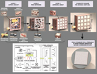
Other military applications stem from the unique electrical properties previously described. For example, the high isolation implies that usual constraints of how close the transmit and receive parts of a communications or radar system can be are no longer limited by the transmission line medium. Another consequence of high isolation is that the coaxial lines can be built in multiple interconnected levels with low-loss sharp 90° turns. This allows a higher density of transmission lines and components as compared to traditional 2D structures such as microstrip and CPW, and provides the freedom of using crossovers wherever needed. Such a simple thing as high isolation coaxial crossovers, highly challenging to do at millimeter wavelengths, enables new products like miniature MxN switch matrices to be realized. In active antenna arrays, for example, electronically-scaned arrays (ESA), the unit cell needs to be smaller than half of a free-space wavelength squared. As the frequency increases to W-band, the wavelength and thus allowed real estate per element scales down faster than the size of the active elements (MMICs). PolyStrata multi-layer technology enables design in the third dimension allowing more functionality for a given footprint. An example of a T/R module for an active array is shown in Figure 5 with the 16-element antenna and all core electrical functionalities included within the profile of 0.64 square centimeters. Such cells could be used alone for tiny high-bandwidth data links or combined into large arrays and digitally steered.
For THz applications, such as radar, imaging and radiometry, coaxial lines become too lossy even if they are TEM, and waveguides become a better choice. For example, at the 0.67 THz minimum of the water-vapor absorption window, a dominant-mode rectangular waveguide is 350 x 160 μm in cross-section. Such RF and LO PolyStrata waveguides and waveguide components are compatible in size with PolyStrata IF micro-coaxial lines, allowing for integrated heterodyne terahertz receivers in the near future.
In conclusion, the new PolyStrata microfabrication technology promises to provide revolutionary improvements in size and performance for existing millimeter-wave systems and produce new components and systems formerly impossible to create. It has already enabled unprecedented improvements in component and system size and electrical performance at high frequencies. The micro-coaxial line technology has demonstrated low loss, low dispersion, low coupling and low parasitic radiation of batch fabricated integrated millimeter-wave components.
Inquiries regarding the technology can be addressed to David Sherrer (dsherrer@rohmhaas.com) or Jean-Marc Rollin (jrollin@rohmhaas.com) at Rohm and Haas Electronic Materials, 3150 State Street, Blacksburg, VA 24060, (540) 552-4610.
Acknowledgments
The authors would like to acknowledge the contributions to this program of Dan Fontaine, Gil Potvin and Rick Thompson of BAE Systems Inc., John Evans of DARPA, Vlad Sokolov and Wendy Wilkins at the Mayo Institute, and the Polystrata team at Rohm and Haas Electronic Materials. This material is based upon work supported by the US Army Research Laboratory under Contract No. W911QX-04-C-0097.
References
1. D. Sherrer and J. Fisher, “Coaxial Waveguide Microstructures and the Method of Formation Thereof,” US Patent US2004/0 263 290A1, December 30, 2004.
2. D. Filipovic, Z. Popovic, K. Vanhille, M. Lukic, S. Rondineau, M. Buck, G. Potvin, D. Fontaine, C. Nichols, D. Sherrer, S. Zhou, W. Houck, D. Fleming, E. Daniel, W. Wilkins, V. Sokolov, and J. Evans, “Modeling, Design, Fabrication and Performance of Rectangular μ-Coaxial Lines and Components,” 2006 Proc. IEEE International Microwave Symposium, San Francisco, CA, June 2006, pp. 1393–1396.
3. K.J. Vanhille, Design and Characterization of Microfabricated Three-dimensional Millimeter-wave Components, PhD Thesis Dissertation, University of Colorado at Boulder, June 2007.
4. M. Lukic and D.S. Filipovic, “Modeling of Three-dimensional Surface Roughness Effects with Application to μ-Coaxial Lines,” IEEE Microwave Theory and Techniques, March 2007, pp. 518–525.
5. D. Filipovic, G. Potvin, D. Fontaine, C. Nichols, Z. Popovic, S. Rondineau, M. Lukic, K. Vanhille, Y. Saito, D. Sherrer, W. Wilkins, E. Daniels, E. Adler and J. Evans, “Integrated Micro-coaxial Ka-band Antenna and Array,” Proceedings GomacTech 2007, Orlando, FL, March 2007.
6. D. Zimmerman, T. Mobley, M. Miller, D. Nair, M. Walsh and M. Smith, “20 to 90 GHz Broadband Characterization of LTCC Materials for Transceiver Modules and Integrated Antennas,” 2006 Proc. of the CICMT-IMAPS Conference, Denver, CO.
7. I.H. Jeong, B.J. Kim and Y.S. Kwon, “Monolithic Implementation of Air-filled Rectangular Coaxial Line,” Electronics Letters, Vol. 36, No. 3, February 2000, pp. 228–230.
8. I. Jeong, S.H. Shin, J.H. Go, J.S. Lee and C.M. Nam, “High-performance Air-gap Transmission Lines and Inductors for Millimeter-wave Applications,” IEEE Trans. Microwave Theory and Techniques, Vol. 50, No. 12, December 2002, pp. 2850–2855.
9. J.B. Yoon, B.I. Kim, Y.S. Choi and E. Yoon, “3D Construction of Monolithic Passive Components for RF and Microwave ICs Using Thick-metal Surface Micro-machining Technology,” IEEE Trans. Microwave Theory and Techniques, Vol. 51, No. 1, January 2003, pp. 279–288.
10. E.R. Brown, A.L. Cohen, C.A. Bang, M.S. Lockard, G.W. Byrne, N.M. Vendelli, D.S. McPherson and G. Zhang, “Characteristics of Microfabricated Rectangular Coax in the Ka-band,” Microwave and Optical Tech. Letters, Vol. 40, March 2004, p. 365.
11. J. Reid and R. Webster, “A 60 GHz Branch Line Coupler Fabricated Using Integrated Rectangular Coaxial Lines,” 2004 Proc. IEEE MTT-S Int. Microwave Symposium Digest, June 2004, pp. 441–444; J. Reid and R. Webster, “A Compact Integrated V-band Bandpass Filter,” 2004 Proc. of IEEE AP-S Int. Symposium, Monterey, CA, July 2004, pp. 990–993.
12. R.T. Chen and E.R. Brown, “An Ultra-compact Low Loss 30 GHz Micromachined Coaxial Filter,” Proc. 35th European Microwave Conference, Paris, France, October 2005.
13. J. Reid, E.D. Marsh and R.T. Webster, “Micromachined Rectangular Coaxial Transmission Lines,” IEEE Trans. Microwave Theory and Techniques, Vol. 54, No. 8, August 2006, pp. 3433–3442.
14. J.R. Reid and R.T. Webster, “A 55 GHz Bandpass Filter Realized with Integrated TEM Transmission Lines,” 2006 Proceedings of IEEE MTT-S International Microwave Symposium Digest, San Francisco, CA, June 2006, pp. 132–135.
15. J.R. Reid and R.T. Webster, “A 6-port 60 GHz Coupler for an RN2 Beamformer,” 2006 Proc. IEEE Antennas Propag. Soc. International Symposium, Albuquerque, NM, July 2006, pp. 1985–1988.
16. E.D. Marsh, J.R. Reid and V.S. Vasilyev, “Gold-plated Micromachined Millimeter-wave Resonators Based on Rectangular Coaxial Transmission Lines,” IEEE Trans. Microwave Theory and Techniques, Vol. 55, No. 1, January 2007, pp. 78–84.
17. I. Llamas-Garro, M. Lancaster and P. Hall, “Air-filled Square Coaxial Transmission Line and Its Use in Microwave Filters,” IEEE Proc.-Microwave Antennas Propagation, Vol. 152, No. 3, June 2005, pp. 155–159.
18. M. Lukic, S. Rondineau, Z. Popovic and D.S. Filipovic, “Modeling of Rectangular μ-Coaxial Lines,” IEEE Microwave Theory and Techniques, May 2006, pp. 2068–2076.
19. K. Vanhille, D.S. Filipovic, C. Nichols, D. Fontaine, W. Wilkins, E. Daniels and Z. Popovic, “Balanced Low-loss Ka-band U-coaxial Hybrids,” 2007 Proc. IEEE MTT-S International Microwave Symposium Digest, June 2007.
20. K. Vanhille, D. Fontaine, C. Nichols, D.S. Filipovic and Z. Popovic, “Quasi-planar High Q mm-wave Resonators,” IEEE Microwave Theory and Techniques, June 2006, pp. 2439–2446.
21. M. Lukic and D.S. Filipovic, “Surface Micromachined, Dual Ka-band Cavity-backed Patch Antenna,” IEEE Transaction on Antennas and Propagation, July 2007, pp. 2107–2109.
22. K. Vanhille, D. Fontaine, C. Nichols, Z. Popovic and D.S. Filipovic, “Ka-band Miniaturized Quasi-planar High-Q Resonators,” IEEE Microwave Theory and Techniques, June 2007, pp. 1272–1279.
Zoya Popovic received her Dipl. Ing. degree from the University of Belgrade, Serbia, in 1985, and her PhD degree from Caltech in 1990. She is the Hudson Moore Jr. Chaired Professor of Electrical and Computer Engineering at the University of Colorado at Boulder. Her research interests include high-efficiency and low-noise microwave circuits, quasi-optical millimeter-wave techniques, smart and multi-beam antenna arrays, intelligent RF front ends, RF optics and wireless powering for batteryless sensors.
Sébastien Rondineau received his PhD degree from the University of Rennes 1, France, in 2002. He was a research fellow at the University of Colorado at Boulder from 2002 to 2006. Currently a research assistant professor at the Microwave and Active Antenna Laboratory, University of Colorado at Boulder, his research interests include the method of analytical regularization in computational electromagnetics, mode matching, conformal mapping, micro-scale interconnects, Butler matrices, propagation and scattering of waves, homogeneous and inhomogenous dielectric lenses, discrete lens arrays and antennas, dispersion-controlled 2D Rotman lenses, nonlinear polymers applied to rectification-modulation for laser, terahertz and microwave signals.
Dejan S. Filipovic received his Dipl. Eng. degree in electrical engineering from the University of Nis, Serbia, in 1994, and his MSEE and PhD degrees from the University of Michigan, Ann Arbor, MI, in 1999 and 2002, respectively. From 1994 to 1997, he was a research assistant at the University of Nis. From 1997 to 2002, he was a graduate student at the University of Michigan. He is currently an assistant professor at the University of Colorado at Boulder. His research interests include the development of mm-wave components and systems, multiphysics modeling, antenna theory and design, as well as in computational and applied electromagnetics.
David Sherrer received his BS degrees in physics and philosophy in 1993 and his MS degree in electronic engineering 1996 from Virginia Tech. He founded ACT MicroDevices Inc. in 1996, which became Haleos Inc. in 2001. Haleos was acquired by Rohm and Haas in 2002 and he has served as the director of research and product development at what is now the Rohm and Haas Microfabrication Center in Blacksburg, VA for the past five years. His interests include product development and commercialization in the areas of advanced packaging, microdevices, microfabrication and advanced materials.
Chris Nichols received his BS degree in physics from Arkansas State University in 1990. In 1992, he received his MS degree in physics from The College of William and Mary. He received his PhD degree in applied science from The College of William and Mary in 1996, where his thesis work involved the engineering of a novel hyperthermal neutral stream etch process tool for charge-free wafer stripping.
Jean-Marc Rollin received his undergraduate degree in material science from Universite d’Orsay in 1998 and his PhD degree in physics from the University of Bath, UK, in 2005. He began his career in 1999 working on packaging and flip-chip assembly technology for high-speed optoelectronic devices at the Corning Research Center, France, from 1999 to 2002. In October 2002, he moved to the department of physics in Bath, UK, where he spent three years of research toward his doctorate, working on millimeter receivers for the British National Space Center. His research interests include the design and fabrication of III-V submillimeter-wave mixers and circuit development.
Kenneth Vanhille received his BS degree in electrical engineering from Utah State University in 2002, and his MS and PhD degrees in electrical engineering from the University of Colorado at Boulder in 2005 and 2007, respectively. He is currently a senior engineer with Rohm and Haas Electronic Materials, Blacksburg, VA. His technical interests include high-frequency packaging techniques, millimeter-wave components and systems, and antenna design.
