In an ever-evolving technological landscape, the optimization of antennas for enhanced connectivity is of paramount importance. This article introduces an approach to leveraging free tools and low-cost equipment to design an IoT device operating from 863 to 928 MHz using antenna boosters. The design process begins by using a library with pre-simulated impedances of antenna boosters on different ground planes of wireless devices. Then, simulation is carried out to impedance match using free software to synthesize a matching network for an antenna booster, considering the topology and actual components, like inductors and capacitors. The circuit simulation even considers the pad layout for component hosting, simplifying the prototyping. Subsequently, a prototype was built and tested with a low-cost vector network analyzer (VNA). This process demonstrates that freeware and low-cost equipment are viable options for designing wireless devices with embedded antenna boosters.
The rapid increase in demand for wireless connectivity in various applications has emphasized the need to optimize antennas for specific environments. For professional applications, antenna systems are simulated with electromagnetic (EM) software and measured with sophisticated equipment, such as VNAs and anechoic chambers. However, freeware and low-cost tools are proposed for early engineering engagement.1,2 This alternative approach engages researchers in designing wireless devices embedding antennas and provides a cost-effective and simplified method for antenna design. These designs can be transitioned to professional tools for more accurate device characterization.
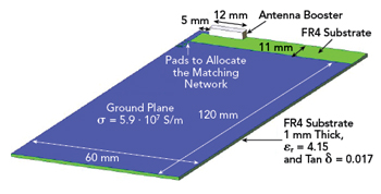
Figure 1 Antenna booster on FR4 ground plane.
To illustrate the simplicity of the design process, a small, non-resonant element will be used in the desired frequency band by modifying the associated matching network.3 This non-resonant antenna booster element measures 12 × 3 × 2.4 mm3. It will be integrated into the FR4 board shown in Figure 1.4
This design procedure is significantly more straightforward than those based on altering the antenna’s geometry.5 For the antenna booster, only the matching network requires adjustment since an antenna booster can be used for many frequency bands and form factors.6 This ease of use is thanks to the non-resonant nature of antenna booster circuit design tools based on matching network synthesis.7 This is a significant advantage as designing a wireless device incorporating an antenna booster can be easily tackled by designing a matching network, which is straightforward, quick and can be entirely addressed by circuit simulation.
Creating a library of devices with different form factors, including antenna boosters, where S-parameters are included over an extensive frequency range, creates the opportunity to simplify the design process. The designer can then select the form factor best suited to the requirements and design the matching network using the library.8,9 Such a library contains pre-simulated S11 data corresponding to different antenna boosters on PCBs of different sizes.
This article details starting with S-parameter data from a library, designing a matching network with another freeware matching design tool and testing the S-parameter data with a low-cost VNA. Since the library has been extensively covered,8 this article focuses on using freeware to design the matching network and measure the S11 parameter with a low-cost VNA. The design flow chart for this process is shown in Figure 2.
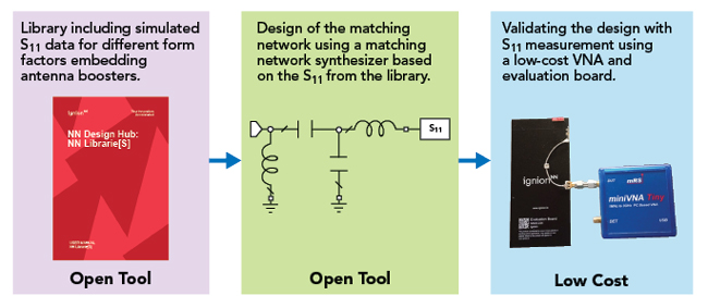
Figure 2 Design flow chart.
Before selecting a freeware matching network design tool, a comparison analysis has been made between the different synthesis tools. The matching network synthesis program must handle complex frequency-dependent impedances and synthesize matching networks with multi-band performance at f1 – f2 and f3 – f4 (for example, 824 to 960 MHz and 1710 to 2690 MHz) and the ability to include real inductors and capacitors with finite Q-factors. Table 1 shows programs addressing these needs.
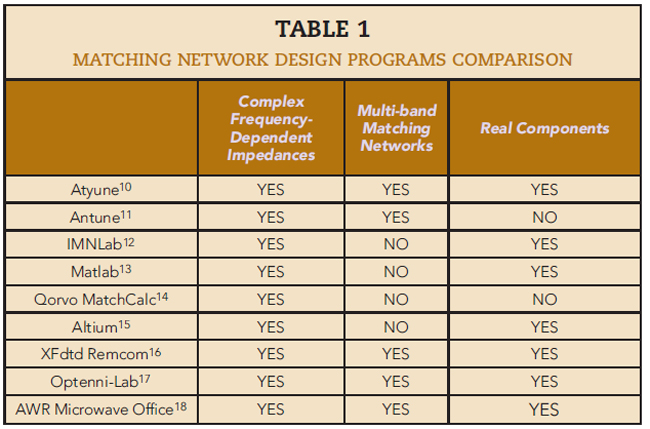
XFdtd Remcom, Optenni-Lab, Cadence AWR Microwave Office and Atyune meet the three criteria in Table 1. The first three software packages offer functionality and are excellent reference tools for professional applications. However, this design uses Atyune because it is an open and easy-to-use tool to synthesize matching networks. It focuses on providing clear and practical guidance to match antennas to specific ground plane dimensions. This software is free to use.
A FREEWARE TOOL FOR MATCHING NETWORK SYNTHESIS
Matching software allows the user to analyze antenna-matching networks. The software will determine parameters like S11, bandwidth, tolerances and matching network efficiency. In addition, these programs can synthesize the matching network for a requirement and specify the components to realize that network.
In this case, the simulations begin with S-parameters from platforms, including antenna boosters, that have been previously simulated. A free library is available from Ignion.8,9 For example, the device in Figure 1 has been simulated with IE3D, an EM full wave solver. This S11 data is available in the library,8 allowing a designer to synthesize a matching network using the flow diagram of Figure 2.
THE NEED FOR A MATCHING NETWORK
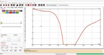
Figure 3 Antenna booster S11 response using Atyune.
The S11 of the circuit in Figure 1 is shown in Figure 3. The S11 performance is poor in the desired 863 to 928 MHz frequency region. The goal is to design a matching network with an S11 value of less than -6 dB.
Efficient matching is essential to optimize system performance and ensure maximum power transfer between the source and load. A mismatch can result in signal reflections and power loss. The results from Figure 3 show S11 = -1 dB at 900 MHz. This means that only 20 percent of the available power is delivered to the antenna system, corresponding to 6.8 dB of mismatch loss. The matching network will match impedances to optimize the source and load. The program will synthesize the topology and components, such as inductors and capacitors, for the desired matching network.
BANDWIDTH POTENTIAL
To optimize the matching network design, the potential bandwidth of the antenna impedance must be analyzed. This step is crucial to determine if the design can provide enough bandwidth. Bandwidth potential allows the designer to estimate the bandwidth even if the antenna is not matched. If the potential bandwidth is larger than the target bandwidth, then a simple matching network with one or two components can be designed to meet the bandwidth requirements. It is important to mention that bandwidth potential can be exceeded when using broadband matching networks. For example, a broadband matching network using an LC resonator can theoretically improve the bandwidth by 2.45 at SWR = 3.19,20,21
The Atyune tool facilitates the efficient evaluation of bandwidth potential. It allows the exploration of configurations and settings directly affecting it, ensuring that the final design meets the desired bandwidth requirements. In the case of the antenna booster in Figure 1, the operating range is 863 to 928 MHz, resulting in a 65 MHz bandwidth. Figure 4 shows the bandwidth potential curve. At 900 MHz, the value is 175 MHz, equating to 19.4 percent, indicating enough bandwidth with an appropriate matching network.
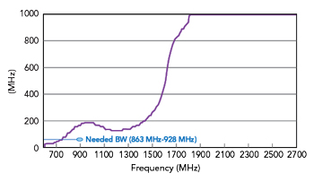
Figure 4 Bandwidth potential at SWR = 3 for antenna booster.
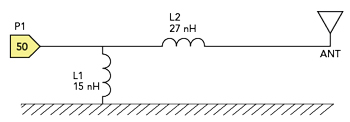
Figure 5 Synthesized matching network.
MATCHING NETWORK DESIGN
Since there is enough bandwidth potential, the program will be used to design a matching network with an S11 of less than -6 dB in the 863 to 928 MHz frequency range. This design will be synthesized to limit the system’s required components. In this case, the matching network contains two elements, as shown in Figure 5. L1 is a 15 nH inductor with a Q of 87 and L2 is a 27 nH inductor with a Q of 89. The program allows real-time adjustments to enable experimentation and optimization.

