The simulated results of the antenna booster from Figure 1, with and without the matching network, are shown in Figure 6. The matching network enables an S11 value from the antenna of better than -6 dB from 810 to 1000 MHz. This 190 MHz bandwidth easily satisfies the 863 to 928 MHz antenna booster frequency range. The 20.9 percent bandwidth of the booster circuit is also close to the 19.4 percent bandwidth potential shown in Figure 4.
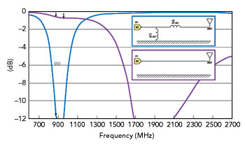
Figure 6 Antenna booster S11 results with and without matching network.
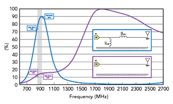
Figure 7 Total efficiency with and without the matching network.
The total matching network efficiency is defined in Equation 1 as:

Where:
ηt = Total efficiency
ηm = Matching efficiency
This antenna booster’s average efficiency is 83 percent over the 863 to 928 MHz frequency range. It should be noted that the total efficiency takes the mismatch and the matching efficiency due to the finite Q of the lumped inductors used in the matching network into account. The total efficiency results for the matched and unmatched antenna booster circuits are shown in Figure 7.
MATCHING NETWORK DESIGN CONSIDERING THE PAD LAYOUT
With the bandwidth and efficiency analysis complete, the next step is to build the board. Before fabricating the board, the size of the lumped component pads and their impact on circuit performance must be considered. Each pad can be modeled by a short transmission line and S11 can be computed. In this case, the pads form an asymmetric coplanar transmission line. The characteristic impedance and effective permittivity can be easily found.3
Figure 8 shows the circuit board layout for this exercise. This layout contains several series and shunt elements to accommodate a variety of circuit configurations. The matching network under consideration requires only Z1 and Z2, so Z3, Z6 and Z7 are shorted, while Z4 and Z5 are left open.
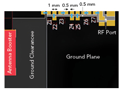
Figure 8 Circuit board layout.
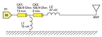
Figure 9 Matching network with actual pads.
The next step is to add the actual pads to the matching network values. This means modeling each pad as a transmission line and determining the impedance, attenuation, permittivity and length characteristics. From Figure 8, Z1 is the 27 nH inductor (L2), Z2 is the 15 nH inductor (L1) and there is a 2 mm transmission line between Z1 and Z2. Since Z3, Z6 and Z7 are shorted together, they are modeled as a 13 mm transmission line. The matching network with actual pad characteristics is shown in Figure 9.
With the actual pads included, the matching network is simulated with L1 and L2 values to analyze the impact of the pads. The result is a 133 MHz, or 15.4 percent, bandwidth from 795 to 928 MHz, where S11 is less than -6 dB. The frequency shifts to lower frequencies because of the inductance introduced by the 2 mm transmission line. These results are shown in Figure 10.
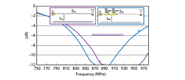
Figure 10 S11 comparison with and without pads.
The next step is to optimize the values L1 and L2 to incorporate the effects of the pad layout. Atyune’s AutoMatching feature will update the initial component values to incorporate the effects of the added pads. After adding the pads, the antenna booster meets the S11 requirements, so no optimization is needed. In other cases, the optimization tool is useful for fine-tuning values to incorporate layout impacts. The simulation results in a bandwidth of 215 MHz, or 23 percent and the design meets the S11 requirements from 825 to 1040 MHz. These results are shown in Figure 11.
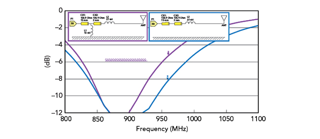
Figure 11 S11 matching network with and without the 15 nH parallel coil.
After careful analysis, it was determined that the 15 nH parallel inductor could be removed. The impedance of this component at 900 MHz is high enough that removing it does not have a relevant effect. Figure 11 shows that the bandwidth of the matching network improves with the inductor removed.

