

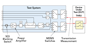
Figure 1 ATS thru measurement.
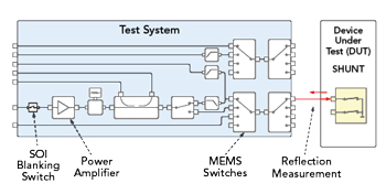
Figure 2 ATS shunt measurement.
It is a perpetual challenge to evaluate the performance of next-generation technology with the current generation of technology. The test industry meets this existential challenge repeatedly by starting with a thorough understanding of the fundamentals that inform test methodology. That understanding guides the selection of technology that will accomplish the task at hand. This is the challenge of characterizing the harmonics and S-parameters of a next-generation, high performance antenna tuning switch (ATS).
Antenna tuning switches are used in broadband antennas to boost the efficiency of the antenna. Since the switches can be placed after the filters in the signal chain, they must be very linear to prevent generating harmonics that are within the passband of the antenna. Given the characteristics of the ATS being tested, the test system must be capable of measuring extremely low harmonic levels, on the order of -140 dBc, with a high-power fundamental signal level of about 10 W. The test system used to characterize the ATS is shown in Figure 1, with the ATS configured for the through measurement and in Figure 2 with the ATS configured for the shunt measurement.
The test system used in both cases is an NI (now part of Emerson) Semiconductor Test System. It generates a high-power signal over an octave bandwidth and 10 W of power. The test signal is routed through a switch matrix to the device under test (DUT) and harmonics generated by the DUT up to 20 GHz are measured. It is desirable to connect to multiple DUTs at once to reduce the test time and test cost per DUT. The switch matrix creates a path from the power amplifier (PA) and receiver to each of the DUTs, separately, during the test sequence. The fundamental tone for harmonic measurements is generated by an NI PXIe-5842 vector signal transceiver and the setup has an NI PXIe-5632 vector network analyzer. This configuration can also perform S-parameter measurements of the DUT in either the shunt or through position.
The conditioning of the test signal begins with the PA, followed immediately by a circulator that provides a path to measure the power reflected due to amplifier mismatch. A forward coupler monitors and can be used to calibrate the output power. Lowpass filters are required to filter amplifier harmonics. A diplexer splits the band between the fundamental and the harmonics. A highpass filter provides additional filtering of the fundamental on the RX side of the diplexer. Because of the signal power, the amplifier and filter components are large and connectorized, requiring cable interconnects and all these factors combine to occupy precious space.
A drawback of having a flexible, multi-DUT connection capability is that it requires multiple switches. This architecture results in a switch tree in the signal path. Since these switches will attenuate the high-power signal, low insertion loss is important and using SP4T switches helps reduce the loss.
Multiple switches create linearity challenges. Each switch generates harmonics that will appear on the test signal and be reflected, affecting the measurement. Finally, a small form factor for the switches is essential to achieve the high connection density that the test system requires.
The methodology for testing high frequency ATS devices puts a burden on the switch. It must handle high power with low distortion, low loss, fast switching speed and have a small footprint. Having a switch that can provide a DC connection is essential as it allows both resistance and leakage measurements of the DUT. The best possible test results are heavily dependent on the switch selection. Selecting the correct component requires a thorough understanding of the available options.
SELECTING THE OPTIMAL SWITCH
A perfect switch has no resistance when biased on and infinite resistance when biased off. It switches instantly, requires no power to change states or to remain on, passes electrical signals from DC to light at any power level, is very small, lasts forever and costs nothing. However, this device does not exist, so switch advantages must be balanced against disadvantages to get as close as possible to the ideal switch. There are two main types of switching technologies used for high frequency applications: solid-state and electromechanical. There are options for each type:
Solid-state:
- Silicon-on-insulator (SOI)
- PIN diode
- GaAs field-effect transistor (FET)
- GaN FET
Electromechanical:
- Relays
- Micro-electromechanical systems (MEMS)
For solid-state switches, PIN diodes are current-controlled and FETs are voltage-controlled. Both can be implemented in different semiconductor processes like GaAs, AlGaAs, GaN and silicon. For FET-based switches, SOI and silicon-on-sapphire are also commonly used.
Using PIN diodes comes with a complex set of tradeoffs. Some of the key advantages are moderate RF power handling of several watts, switching speeds in the nanosecond to microsecond range, high isolation and IP3 values that can be greater than 45 dBm. Those advantages must be weighed against the disadvantages of DC power consumption that may exceed 100 mW per switch, low frequency operation that may not go below 50 MHz, larger overall circuit area and increased insertion loss created by additional passive bias components.
GaAs FET-based switches easily cover the desired frequency range and are widely used. GaAs FETs have switching speeds in the nanosecond range for 10 to 90 percent settling. That is sufficient for many systems, but gate lag can amount to several milliseconds. This decreases the usefulness of GaAs devices in precision test and measurement applications requiring signal stability and complete settling. GaAs switches suffer from lower RF power handling, typically in the 0.5 W range with higher insertion loss, especially for high throw count switches. The linearity is mediocre with IP3 values around 35 dBm and low P1dB performance.
GaN switch performance is similar to GaAs, but these devices can typically handle much higher RF power levels. GaN switches need control voltages in the 40 to 60 V range. Most GaN switches are also limited, in general, to a maximum operating frequency of 18 GHz. They also have similar switching characteristics to GaAs switches, including gate lag and they are generally more expensive.
Newer SOI devices are now gaining favor over commonly used GaAs switches because they exhibit much higher linearity and can provide Class 1C or greater ESD protection. However, higher operating frequencies require smaller devices, which affects the power handling of the switch. While the linearity of SOI switches is much higher than other solid-state switch technologies, it is still insufficient for many applications, including testing an advanced ATS.
Electromechanical (EM) relays work from DC to 50 GHz and beyond with minimal insertion loss, good return loss and high isolation. They can handle hundreds of watts and have extremely high linearity. However, EM switches consume hundreds of milliwatts of DC power when actuating, have switching speeds in the tens of milliseconds and are physically large, heavy and expensive. They also have comparatively short lifespans.
CHOOSING MEMS
After thoroughly evaluating various switches, MEMS switches stand out as the best choice. MEMS switches combine the performance advantages of EM switches with the miniature size, low cost, long life and scalability of solid-state switches. Ohmic MEMS switches operate by applying a DC voltage to the gate electrode. With no gate voltage, the beam is in its resting position as shown in Figure 3a. When the voltage applied to the gate reaches the pull-in voltage, the beam or cantilever bends toward the contact due to electrostatic force and connects the input to the output, as shown in Figure 3b. When the DC voltage falls below a pull-off level, the beam returns to its original position under its spring force. It is important to mention that while the pull-in voltage is in the tens of volts (DC), no power is consumed by the switch during actuation.
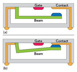
Figure 3 (a) Ohmic MEMS switch in the open position. (b) Ohmic MEMS switch in the closed position.
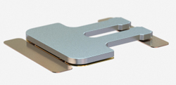
Figure 4 Menlo Micro’s single unit cell ohmic cantilever design.