

The Ideal Switch® from Menlo Micro is an ohmic cantilever design. The terminals of this MEMS switch can be viewed as a gate-source-drain transistor. In its simplest configuration, the switch is a single-beam, three-terminal device, acting as an SPST relay. This resembles an EM relay, but a MEMS switch is microscopic. The minimal size is highly advantageous. This 50 × 50 μm unit cell element, shown in Figure 4, can easily be scaled into countless switching configurations with multiple throws and poles.
An SP4T MEMS switch from Menlo Micro was selected to meet the ATS test requirements. The device is shown in Figure 5 in a glass wafer-level chip scale package. It was selected to take advantage of its small size, low loss, extremely high linearity and power handling performance. This switch has a single pole in the center of the die and four throws in the corners. Note that each arm of the switch is constructed from four parallel branches of unit cells to reduce the loss and increase its power handling.
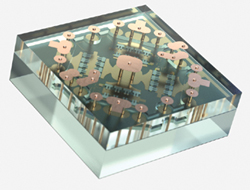
Figure 5 The Menlo Micro MM5130 SP4T switch.
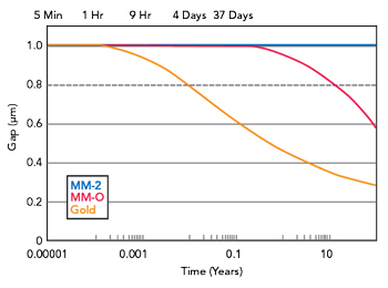
Figure 6 Switch deformation.
A key to power handling and reliability is the proprietary electrodeposited alloys, which have mechanical properties similar to silicon with the conductivity of metal. These alloys exceed gold for strength and creep resistance. The specialized cantilever of the device design leads to longer life performance as indicated by the data shown in Figure 6. This accelerated life test data shows how the initial 1 μm gap between the cantilever and the output contact collapses over time for a gold cantilever as compared to cantilevers manufactured with Menlo Micro’s MM-0 and MM-2 alloys. In this case, the failure criterion is a gap below 0.8 μm. Note that the gap with MM-2 remains practically unchanged for well over 20 years.
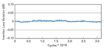
Figure 7 Contact cycling with 10 dBm input at 25°C.
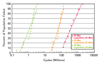
Figure 8 MM5130 hot switching.
The materials used to provide stable and consistent contact performance over switch cycling and temperature are another critical aspect of this device. The switch uses a Ruthenium alloy along with a controlled atmosphere, which results in reliable operation for billions of cycles, as seen in Figure 7, where insertion loss variations were monitored as the device was cycled. Note that the insertion loss was measured with an RF power of 10 dBm, indicating excellent reliability even with low levels of hot switching. Higher levels of hot switching are also possible if reduced life is acceptable as is evident from the measured data in Figure 8. This plot shows the expected life of the switch when switching up to 30 dBm of RF power. Lifetimes of millions to hundreds of millions of cycles are achievable even with moderate levels of hot switching.
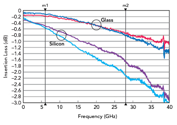
Figure 9 Insertion loss comparison of different substrates.
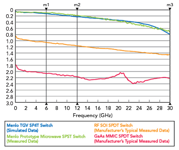
Figure 10 Insertion loss of different switch technologies.
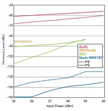
Figure 11 Second and third harmonic performance of different switch technologies.
The Ideal Switch utilizes a through-glass via (TGV) process that enables a bumped, wafer-level chip scale package with a 2.5 mm × 2.5 mm form factor. The glass substrate is an important part of the performance improvement of the switch. Figure 9 compares two SPST MEMS switches on glass with two switches on high-resistivity silicon substrates. The switches on the glass substrates show an improvement in loss of roughly 0.5 dB at 6 GHz and approximately 1 dB at 28 GHz. Figure 10 shows an insertion loss comparison between the SP4T Ideal Switch, an SPDT SOI switch and an SPDT GaAs switch.
A glass substrate has additional benefits. It provides higher linearity than SOI switches that are built on high-resistivity silicon because it is a better electrical insulator and not a semiconductor. For reference, the IP3 of Menlo Micro’s switches is typically greater than 95 dBm. The glass substrate also provides thermal stability that allows the electrical performance of the switch to remain unchanged over a temperature range of -55°C to +85°C. The harmonic performance of several different switch technologies is shown in Figure 11.
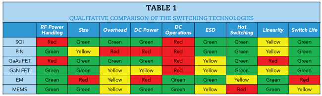
Table 1 shows the advantages and disadvantages of the different switch technologies for a variety of characteristics. While no technology is perfect, MEMS switches offer substantial benefits for a test system. The small size allows a large switch matrix to connect multiple DUTs. The low insertion loss reduces the RF power dissipation, maximizing the receive signal level. Although hot switching is a disadvantage of the MEMS switch technology, the Ideal Switch used in the test setup performs better than other MEMS switch offerings and the test system can control the test signal to avoid hot switching. The MEMS switch allows DC parametric measurements and the switching characteristics reduce test times.
USING MEMS IN ATS TESTING
Having settled on the switch, there are still testing challenges to address. The nominal HPA power is 10 W, corresponding to a peak voltage of almost 32 V into 50 Ω. The presence of an open or short, caused by the DUT or a problem in the path, can almost double the peak voltage. The component specifications must be checked against this worst-case peak voltage possibility. It is possible for components to handle the nominal power level but be underrated for the peak voltage experienced in a short or open condition. From here, the DC testing is relatively straightforward. The test voltage is less than one volt and the current is measured with a high-quality source measurement unit.
A minor drawback of MEMS switches is the presence of a shunt resistance when the switch is closed in addition to the shunt resistors required to prevent floating nodes. A simple calibration is required to accurately measure the resistance. The DC path also provides a simple and fast way to measure the continuity of the switches as a self-test to ensure the path is complete.
Since hot switching degrades the lifetime of a MEMS switch, test system techniques become important. Typically, a programmable device will ensure the RF input is disabled whenever a switch changes state. Developing a test system that allows control of the RF input is critical when using MEMS switches. In addition to the hot switching issue, many DUTs do not have appropriate heat sinks. To minimize these thermal issues, the duty cycle of the test may be adjusted to prevent overstressing the DUT.
Frequency harmonic levels for DUTs may be quite low, on the order of -120 dBc. In addition to the DUT, any active element in the test path will generate harmonics. As seen in Figure 11, this is a strength of the MEMS switches. The test system harmonic performance must be much better than the DUT being tested to prevent effects that will impact measurement accuracy.
CONCLUSION
The use of ATS in wireless systems is increasing. As the opportunities grow, the performance requirements get more difficult and this means test system performance must keep pace. Incorporating MEMS switches, along with a complex software framework into NI test systems is enabling the evolution of testing. Systems using these components and concepts have been successfully incorporated in production settings where these systems are providing the performance required to test leading-edge ATS products. Challenges remain, but architectures and configurations will evolve in response and MEMS switches will remain a vital part of this evolution.