

Phased arrays, more formally known as active electronically steerable arrays (AESAs), are a popular architectural choice for radar, 5G and 6G base stations, satellite communication platforms and mobile device applications. When optimized, beamforming via phased arrays improves signal quality, data throughput and user experience. As array sizes grow, so does the difficulty in designing and optimizing antenna elements and signal processing. Physical evaluation in anechoic chambers can take weeks and setups striving to represent real-world conditions may be incomplete, tenuous or infeasible. The alternative is simulating phased array designs quickly, inexpensively and accurately reproducing behaviors and effects in virtual space.
System-level simulations with measurement-based models, authentic modulation at full bandwidth, circuit and electromagnetic (EM) co-simulation, cross-domain analysis and other techniques can reproduce complex scenarios accurately and inform design optimizations. However, high-fidelity simulation comes with computational costs and with phased arrays scaling into the hundreds and soon, thousands of elements, simulation time becomes a concern. Adding to the phased array analysis complexity are effects associated with array active impedance, where elements couple and interact under array excitation.
Array active impedance is receiving increased attention from electronic design automation (EDA) researchers at Keysight. Teams approach real-world problems in three phases: developing models via measurements or simulations, testing the accuracy of those models in simulations with real-world conditions and then generalizing models and simulations to evaluate more complex applications at scale.
Phased array design is an example of how this approach to EDA research pays off. A behavioral simulation methodology using Keysight SystemVue decomposes large phased arrays with their signal processing chains into smaller tiles for S-parameter coupling matrix extraction, then stitches tiles together with element remapping to represent the entire array with active impedance effects in fast, accurate virtual analysis. This article will explore this more efficient methodology in four parts, including a first look at a patented technique for building the required full-array S-parameter matrix from a smaller matrix:
- Accurate array behavioral modeling from measured or EM-simulated embedded element patterns
- High-fidelity modeling of power amplifiers (PAs) under load-pull conditions
- Iteratively capturing array active impedance with beamforming applied
- Extending far-field pattern simulations from smaller to larger phased array systems.
ACCURATE ARRAY BEHAVIORAL MODELING FROM MEASURED OR EM-SIMULATED EMBEDDED ELEMENT PATTERNS
Traditionally, designers measured antenna elements to understand patterns. Advances in circuit/EM co-simulation techniques using ADS in the workflow provide a faster, less expensive way to predict phased array element behavior before fabricating physical devices. Figure 1 shows a layout of a 4 × 8 array in ADS for EM simulation with Keysight RFPro.
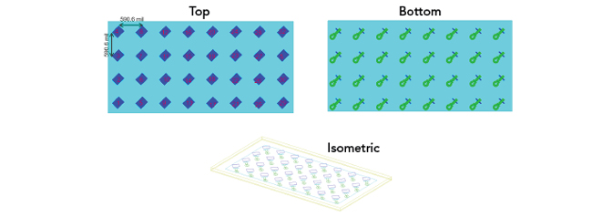
Figure 1 Antenna array layout in ADS.
RFPro simulation produces an embedded element pattern in a .ffio file by automatically exciting the entire array one element at a time with all other element ports terminated, capturing the pattern of every element in its position in the array. Element patterns differ depending on metallization, structural details and position of the element in the array. Elements also exhibit EM coupling, where energy radiated from one element is picked up by others. Modeling this mutual coupling is essential to accurately predicting far-field patterns of an array. The simulation also produces an S-parameter matrix representing the entire array.
A SystemVue model of an array starts with an antenna configuration preserving the exact mapping of numbered element locations corresponding to the ADS layout. Then, the embedded element pattern and the S-parameter matrix are imported. Figure 2 shows a simple schematic for the 4 × 8 array and import dialogs to complete the configuration.
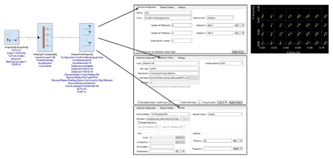
Figure 2 Importing the element pattern and S-parameter matrix from the SystemVue schematic.
Moving from a detailed EM simulation to a behavioral simulation loses little to no fidelity, as shown in the boresight pattern plots in Figure 3. However, the computational reduction is significant. EM simulation of the whole array is feasible for small arrays. However, as element counts increase toward 100 and beyond, effect complexity increases and the advantage of reduced behavioral simulation time becomes apparent, becoming even more so with simplifications to array models discussed shortly.
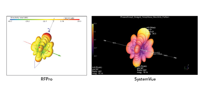
Figure 3 Boresight pattern plots from EM (RFPro) and behavioral (SystemVue) simulations.
HIGH-FIDELITY MODELING OF PAS UNDER LOAD-PULL CONDITIONS
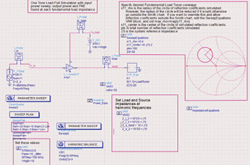
Figure 4 Load-pull analysis for a PA using a harmonic balance simulation in ADS.
RF PA design is an excellent example of how multi-variable optimization becomes necessary. Designers look at gain, peak and average power delivery and efficiency, distortion, linearity, noise and other performance metrics across a given bandwidth. Changing any feature of a PA typically affects several metrics. Circuit/EM co-simulations can sweep a set of parameters simultaneously and optimization techniques can explore a multi-dimensional surface and look for the best results.
Load-pull analysis provides deeper insight into PA performance when drive impedance, the load the amplifier sees, varies. Low frequency PAs usually define a fixed resistive termination as the load, such as 50 or 75 Ω, creating an operating point for optimization. Changing drive impedance pulls the PA away from its intended operating point, often unpredictably, with cross-domain interactions.
Figure 4 shows a load-pull analysis for a simple one-amplifier schematic in ADS. Harmonic balance simulation uses a single tone plus harmonics with swept input power and different load impedances at harmonic frequencies. The simulation exposes PA distortion and non-linearity while capturing gain, output power and power-added efficiency at each load impedance. Also plotted in Figure 4 is a Smith chart with a contour indicating shifts in the PA’s S-parameters as the load changes.
In a phased array design, loads on PAs in each element’s signal processing chain change continuously due to the effects of array active impedance. This makes the behavioral characterization of a PA with load-pull effects incorporated imperative. Load-pull analysis with circuit/EM simulation in ADS results in changes to the PA’s X-parameter matrix describing its behavior.
Importing the load-pull enabled PA X-parameter matrix into SystemVue provides a high-fidelity PA model for more accurate behavioral simulation. Each element in the phased array has a complete RF signal processing chain with PAs and other components such as phase shifters. With insight from a load-pull analysis, one optimized chain needs replication for the number of elements in the array. Smart models help condense a set of these chains into a single line. Figure 5 shows the behavioral model for an 8 × 8 phased array.
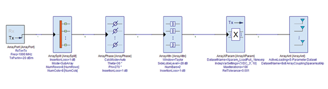
Figure 5 Architectural view of an RF signal processing chain in SystemVue.
Following the methodology described so far, this simplified phased array behavioral model now contains antenna patterns for each element. It also includes basic EM coupling effects between elements and load-pull effects on the PAs behind each element. While this adds significant fidelity to the model, two more steps are needed to accurately capture real-world phased array behavior.
ITERATIVELY CAPTURING ARRAY ACTIVE IMPEDANCE WITH BEAMFORMING APPLIED
Phased arrays have one fundamental purpose: beamforming. This is the process of steering and shaping a beam for its context. In radar systems, a wide beam offers faster detection, with narrower beams used to track one or more targets after acquisition. In 5G and 6G systems, beamforming at the base station and mobile device creates massive MIMO connections for optimum data throughput. Satellite systems apply beamforming to improve link margin and overcome channel interference.
Beamforming uses a phased array or one or more subsets of its elements to create beams with specific directions and shapes. In addition to the raw EM coupling between elements due to layout and structural issues, the weight, steering angle and phase shift of a beam applied to the array or a subarray results in each element presenting active impedance. Two time-varying effects ensue: a load-pull effect on the PAs with mutual coupling effects across elements. These simultaneous effects, more complex than found in the separate analyses of the elements and PAs, alter the intended shape of a beam.
After developing detailed models with frequency-domain simulations, fully uncovering array active impedance effects on far-field patterns requires time-domain simulation with representative beamforming stimuli. Figure 6 shows the XParam model in the data flow used to simulate phased array systems containing amplifiers described with X-parameters files with load-pull information and to model antenna active impedance.
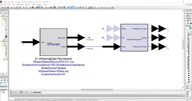
Figure 6 Adding array active impedance with an XParam model in the time-domain data flow simulation.
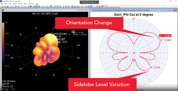
Figure 7 5G NR beam orientation change with array active impedance enabled.
First, the time-domain simulation generates a beam steered at a 30-degree angle with only an imported X-parameter model for PA load-pull. For the next step, the simulation imports the antenna element patterns and the element coupling matrix and enables active impedance. Figure 7 shows a phi cut plot indicating a two-degree shift in the beam angle and significant sidelobe level variation with active impedance enabled.
Simulation users see only a “yes/no” switch to enable active impedance in the analysis. Behind the scenes in SystemVue are calculations using X-parameter representations of the PAs and the coupling matrix of the antenna elements. The challenge is that PA load impedance values depend on knowing the reflection coefficients of the antenna ports. These values are unknown initially, preventing sequential calculation. Simulations work iteratively to converge incident and scattered voltage waves into and out of the PAs and the element reflection coefficients. Then, the time-domain data flow simulation calculates the actual impedance seen by each of the PAs, including the coupling effect between elements. Also, enhancements to data storage streamline the iterative calculations searching for PA operating points, avoiding repeated passes where amplitude and phase values are the same as in prior passes.
Time-domain analysis innovations position phased array designers to have more accurate insight into system-level performance, especially far-field patterns, than previously possible with only frequency-domain analysis. Still, as array sizes grow, S-parameter matrices expand, driving simulation times exponentially higher. A simplification of the array representation reins in simulation complexity while retaining behavioral model fidelity.
EXTENDING FAR-FIELD PATTERN SIMULATIONS FROM SMALLER TO LARGER ARRAYS
Keysight researchers observed that circuit/EM co-simulation time starts becoming uncomfortably long at around 100 unique elements, such as in a 10 × 10 array. This raised the question of whether building larger arrays from smaller ones would be possible in virtual space, avoiding long simulation times by leveraging detailed analysis of fewer elements and signal chains and accurately extending those behaviors to other elements in the model. U.S. Patent 11,921,144 describes such a method directly applicable to system-level behavioral simulations.
The idea of scaling from smaller arrays begs the question: are all individual element behaviors in larger arrays unique? Empirical analysis shows that each element displays significant EM coupling with adjacent elements and some coupling with elements two places away in any direction. After a two-element distance, coupling diminishes to insignificance. The two-element coupling distance observation suggests the minimum array size for detailed active impedance analysis should be 5 × 5, where the coupling of each element is unique. A 5 × 5 array is convenient for illustration purposes, but other odd array sizes, such as 7 × 7 or 9 × 9, work with the method about to be described.
Figure 8 begins on the left with a 5 × 5 subarray and 25 uniquely-numbered elements. Element 13 is coupled to every other element since all are within a two-element distance, while Element 1 couples to only eight as a boundary condition. A naïve assumption would tile 5 × 5 subarrays to reach bigger uniform rectangular array sizes. However, with EM coupling between elements considered, simple tiling creates discontinuities, violating coupling behavior at the subarray boundaries. Element 1 in the upper right subarray in the middle of Figure 8, as analyzed in the 5 × 5 subarray, does not expect to couple with elements to its left, with the same being true for Element 21 in the upper left subarray looking to its right.
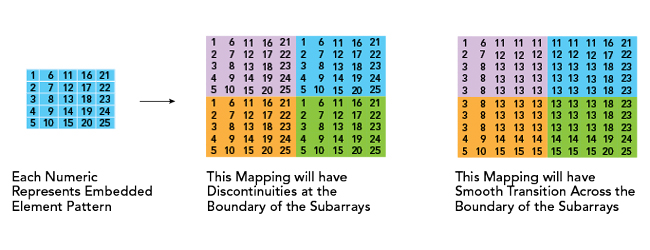
Figure 8 Remapping 25 elements from a 5 x 5 array into a 10 x 10 array.
Boundary conditions need addressing if tiles are to scale without repeating detailed analysis. Moving into a 10 × 10 array, remapping array elements starting from their positions in the 5 × 5 subarray solves the edge discontinuities. Each element is no longer unique and coupling in the full 10 × 10 array is accurately represented using only the 25 elements from the 5 × 5 array. Element 13 repeats in the remapped 10 × 10 array on the right of Figure 8, where the two-element coupling distance in any direction applies. Similarly, other elements repeat with their coupling relationships in the 5 × 5 subarray preserved.
Exhaustive analysis of the 5 × 5 subarray with load-pull and EM coupling recognized results in accurate S-parameter properties for each of its 25 elements. Simplifying the 10 × 10 array with 75 percent fewer unique elements by mapping their associated S-parameter properties into a larger S-parameter matrix provides significant gains in simulation time and the savings grow with even bigger arrays. The method also preserves fidelity; simulations of 10 × 10 arrays with simplified remapped elements agree to four decimal places with simulations of 10 × 10 arrays using 100 unique elements. Generalizing the technique allows designers to model phased arrays of hundreds or even thousands of elements.
ENABLING ITERATIVE PHASED ARRAY DESIGN IN ONE VIRTUAL WORKFLOW
Phased array designers may have had a qualitative understanding of array active impedance but not an effective way to quantify it without lengthy trial-and-error cycles of measurements, design adjustments and hardware re-spins. Fortunately, behavioral simulation technology and modeling advancements have caught up. They provide a shift left to accurate results in virtual space earlier in the phased array design cycle.
Simplifying system-level behavioral modeling for efficient simulation of phased arrays is a significant breakthrough. The crucial addition of time-domain data flow simulation capability and the insight into remapping elements enables designers to spend more time calibrating and optimizing the design of the array elements and RF signal processing chains. These techniques also allow quick iterations of simulations to confirm results, even as phased array sizes scale much larger.