

This article presents a novel substrate-integrated waveguide (SIW) diplexer with high isolation and high-frequency selectivity based on electromagnetic perturbation technologies. The capacitive perturbation and magnetic coupling between the non-resonant nodes (NRN) and the even mode are introduced in dual-mode duplexers. Moreover, two transmission zeros on both sides of each passband can improve the frequency selectivity of each channel of the duplexer and the isolation between the two channels. Furthermore, the zero-degree feeding technology with the microstrip line T-junction has been adopted in the presented diplexer, further reducing the circuit size and improving the isolation. The designed diplexer, centered at 5 GHz and 5.25 GHz, has been simulated, fabricated and measured. It exhibits an isolation of greater than 45 dB and the measured results are in good agreement with the simulated ones.
Researchers pay attention to diplexers that can realize important functions such as filtering and frequency selection. These characteristics are very important for optimizing frequency resources, protecting channels and improving communication quality. Wireless communication systems require diplexers with high performance, especially in applications requiring high isolation, high-frequency selectivity, miniaturization and high levels of integration.
SIW has been widely used as a planar waveguide structure in the design of microwave and millimeter wave passive circuits, such as filters,1-3 power dividers4,5 and couplers6,7 because of integration capabilities, a high quality factor and low cost. Based on the advantages of SIW, many researchers have proposed SIW for dual-mode resonator diplexers.8-13 A dual-mode resonator is commonly used in a design to miniaturize circuits. Besides reducing the number of resonators, this approach improves the flexibility and performance of the design. However, conventional SIW T-junctions in SIW diplexers are typically large. Many designs have been proposed to reduce the circuit size while maintaining good performance. In research,14-16 microstrip T-junctions have been employed and studies17 have introduced SIR (stepped impedance resonator) circuits that remove the T-junction and greatly reduce the circuit size. Research18 introduced a fractal geometry concept in CRLH (composite right/left hand) transmission line designs, using only one CRLH cell to achieve broadband harmonic suppression and frequency selectivity. In addition, several novel microstrip line diplexers have also been investigated.19-21 It is also worthwhile to note that tunable diplexers have been proposed as wireless communication systems move towards more functionality and higher levels of integration.22
This article presents a compact SIW diplexer with two channel filters. SIW dual-mode resonators are utilized for the diplexer’s channel filters to reduce the number of resonators and miniaturize the diplexer. The SIW dual-mode resonator has two different circuit coupling topologies. One topology is perturbation coupling11,23 and the other is NRN coupling.15,24 The two topologies can produce two transmission zeros on both sides of the passband. Furthermore, the diplexer adopts zero-degree feeding technology with the microstrip line T-junction, further reducing the circuit size and improving the isolation.
ANALYSIS OF THE SIW DUAL-MODE RESONATOR
Two degenerate modes of the SIW rectangular resonator, TE102 and TE201, are used to design the SIW dual-mode-resonator diplexer. The resonant frequency, fm0n, of the TEm0n mode of the SIW resonator is given by Equation 1:5
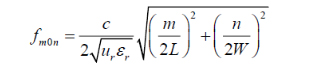
Where:
c is the velocity of lightL is the length of the resonator W is the width of the resonator
For this article, the resonator dimensions can be calculated from Equation 1 as L = W = 36.8 mm when the permittivity, εr, equals 3.5 and the resonant frequency is 5 GHz.
Figure 1a shows the perturbation coupling topology of the SIW dual-mode resonator and Figure 1b shows the NRN coupling topology for that same resonator. S and L in the diagrams represent source and load, respectively. The operating mode in resonator 1 is the TE102 mode (odd mode), while the operating mode in resonator 2 is the TE201 mode (even mode). Resonator 3 represents the NRN.
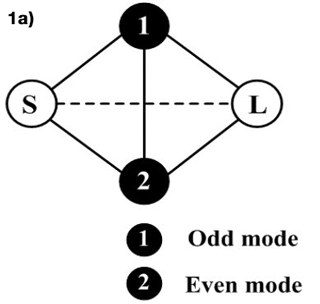
Figure 1a Perturbation coupling topology of the SIW dual-mode resonator.
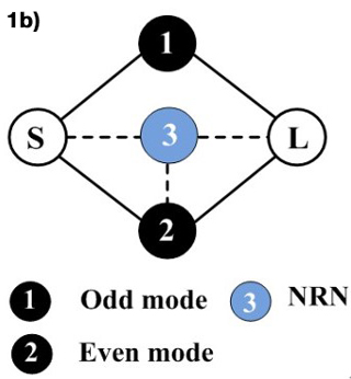
Figure 1b NRN coupling topology of the SIW dual-mode resonator.
The perturbation coupling topology can realize the split of two degenerate modes. The perturbation changes the odd-mode frequency while energy couples with the even mode. The NRN coupling realizes a dual-mode filter. The NRN coupling greatly impacts the circuit's performance because the energy coupling between the NRN and the even mode can produce two transmission zeros without increasing the order of the filter. In practical filter design, the transmission zeros are generated in the real frequency axis so that the frequency selectivity of the passband can be improved. The topology shown in Figure 1a adopts a capacitive perturbation structure. The topology shown in Figure 1b adopts the even mode due to the magnetic coupling between the NRN and the even mode. Both structures can generate two transmission zeros in the real frequency axis and the frequency response of the capacitive perturbation coupling and magnetic coupling with the NRN of the dual-mode resonator is shown in Figure 2.
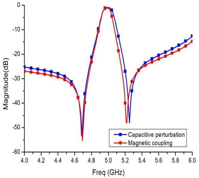
Figure 2 Frequency response of the dual-mode resonator.
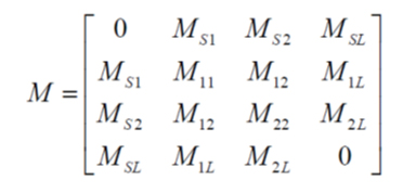
The corresponding coupling matrix, M, for the circuit coupling topology of Figure 1a can be written as Equation 2 and the coupling matrix for the topology of Figure 1b as Equation 3:
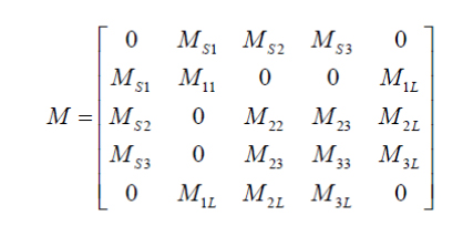
Where:
MS1 is the coupling between the source and resonator 1
MS2 is the coupling between the source and resonator 2
MS3 is the coupling between the source and resonator 3
M1L is the coupling between resonator 1 and the load
M2L is the coupling between resonator 2 and the load
M3L is the coupling between resonator 3 and the load
M12 is the coupling between resonator 2 and resonator 1
M23 is the coupling between resonator 3 and resonator 2
MSL is the coupling between the source and the load
The above analysis requires capacitive perturbation and magnetic coupling between the NRN and the even mode. Figure 3a shows an H-type capacitive perturbation slot where the electric field of the TE102 mode (odd mode) is strongest. Figure 3b shows a co-planar waveguide (CPW) located where the electric field of TE201 mode (even mode) is strongest. This is the NRN structure. The magnetic coupling between the NRN and the even mode is evident. It can be seen that the H-type slot mainly changes the electric field distribution of the odd mode. The magnetic coupling between the NRN and the even mode is primarily realized by using the CPW and the effect on the odd mode can be neglected by proper selection of the location of the slot.
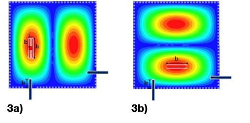
Figure 3a Capacitive perturbation coupling circuit.
Figure 3b Magnetic coupling with the NRN.
The passband width can be controlled for the proposed structures by adjusting the capacitive perturbation and magnetic coupling between the NRN and the even mode. For the coupling structure shown in Figure 3a, the perturbation to the odd mode can be changed by changing l1. As shown in Figure 4a, larger l1 values create more odd-mode perturbation, increasing the passband. Similarly, for the coupling structure shown in Figure 3b, the magnetic coupling between the NRN and the even mode will change with varying l3. As shown in Figure 4b, increasing l3 increases the magnetic coupling between the NRN and the even mode, increasing the passband. Therefore, second-order, dual-mode channel filters can be realized by reasonably controlling the capacitive perturbation or the magnetic coupling between the NRN and the even mode.
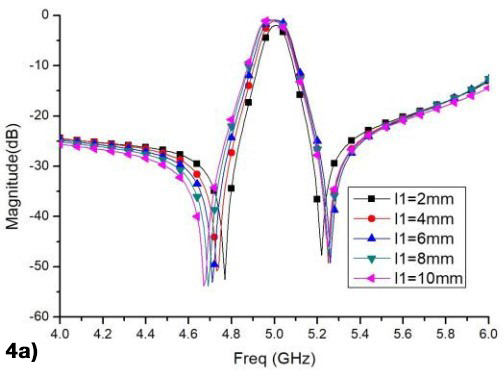
Figure 4a Passband frequency response varying l1.
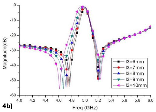
Figure 4b Passband frequency response varying l3.