This article describes a microstrip log periodic dipole array (MLPDA) antenna operating over S-, C-, X- and Ku-Bands that employs a tapered balun feed structure. The antenna has good input-matching characteristics and end-fire radiation performance over the 2 to 18 GHz operating band with an average peak gain of 6.2 dBi. It is cost-effective and compact without the need for complicated or loaded structures.
Log periodic dipole array (LPDA) antennas have been employed in wireless communication systems since their invention in 1957 by DuHamel and Isbell.1 The conventional LPDA is well-suited for applications requiring bandwidth up to a decade, an end-fire pattern and reasonable gain. MLPDA antennas are good candidates for use in modern communication devices as they are easy to fabricate, are low-cost, have low power consumption and are also suitable for integration with microwave integrated circuit modules.2
LPDA antennas printed on an electrically thin dielectric substrate were first introduced by Campbell et al. in 1977.3 Since then, considerable research has been conducted using various techniques to increase bandwidth, reduce size, improve front-to-back ratio, lower the cross-polarization level and increase gain.4,5 However, the impedance bandwidth of microstrip antennas is inherently narrow and designing an MLPDA antenna that provides stable radiation characteristics over a wide bandwidth is challenging.
Recently, several solutions have been proposed to solve this problem. Yang et al.6 fed the antenna with a half-mode substrate integrated waveguide with added metal plates. Chu et al.7 used a similar technique with a bow tie parasitic cell for 5G. The complexity associated with this type of feed is its main disadvantage. Yang et al.8 adopted a feed approach with double-sided parallel stripline from the backside operating in the 2.5 to 6 GHz frequency range. The drawback is that this requires a four-layer circuit board for antenna construction. Hereth et al.9 investigated the use of dipole trimming and parasitic elements in the 3.4 to 9.5 GHz band but the addition of the parasitic elements increases the antenna size. Although these designs enhance antenna performance in general, bandwidths remain relatively narrow and the designs could only be realized with specialized technologies.
A simple feed was proposed by Abutarboush et al.10 This solution proposes a flexible MLPDA antenna on an ultra-thin DuPont™ Kapton® film substrate with a paired CPW parallel strip combination connected through a conductive via. Casula et al.11 suggested the same feed method, but this technique did not significantly improve bandwidth.
Compared to the previous feed techniques, a tapered microstrip balun is relatively easy to fabricate and connect to external SMA connectors. In addition, it offers the potential for wideband impedance matching.12-14 This work demonstrates a wideband 2 to 18 GHz MLPDA antenna with an integrated balun transformer. In this approach, the feed transitions from a microstrip line to a double-sided parallel stripline. CST Studio is used for preliminary numerical studies to obtain an optimal design before fabrication and measurements.
ANTENNA DESIGN

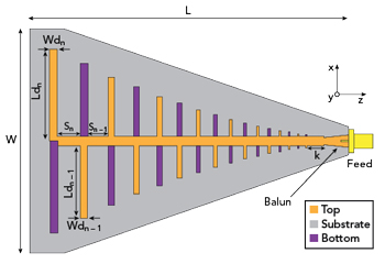
Figure 1 Antenna geometry.
The structure is like a standard, wire LPDA and it uses a typical LPDA design strategy.15 The LPDA antenna is shown in Figure 1. It comprises a set of dipole elements alternately printed on both sides of a microstrip substrate that is fed with an SMA connector to match the 50 Ω input impedance.
The resonant frequency of each dipole element changes periodically in conjunction with a logarithmic function related to the dipole size. Given N dipole elements:
Ldn = Length of the dipole element dn
Wdn = Width of the dipole element dn
Sn = Inter-element spacing between two adjacent dipoles
WL = Width of the microstrip feed line
LL = Length of the microstrip feed line
K = Feed length
These geometrical parameters must be properly tuned to realize a working antenna.
For a given desired bandwidth, where fmin and fmax are lower and upper cutoff frequencies, the design starting point is the definition of the parameters α, τ and σ considering the empirical rules defined by Milligan.16
The aperture angle α is given by Equation 1:

The scaling factor, τ, which is the ratio between lengths of two consecutive dipoles, Ldn and Ldn-1, is the most important design parameter. This relationship is shown in Equation 2:

The spacing constant σ is given by Equation 3:

The desired operating frequency range with upper and lower truncation constants, t1 and t2, determined for τ and σ are combined to compute the length of the longest element and determine the number of elements required. The longest element length is given by Equation 4:

where λ1 is the longest operating wavelength and t1 is determined empirically from Equation 5:16

The upper truncation t2 constant is defined as shown in Equation 6:

The truncation constants and the frequency band determine N as shown in Equation 7:

To determine the widths of the dipole elements and the feed line, the first assumption is that the required input impedance is real. The average characteristic impedance Z0 of the cylindrical dipole is given in Equation 8:17

where an = radius of the equivalent cylindrical dipole.
The width of the longest printed microstrip dipole element is approximatively equal to the perimeters of the cylindrical dipole as determined by Equation 9:3

After determining the length and width of the largest dipole element from Equation 4 and Equation 9, the lengths and widths of the remaining dipoles Wdn and Ldn for n = 1, 2, 3…N-1 are calculated by iterating the scaling factor τ.

