

2 to 18 GHz MLPDA Employs Tapered Balun Feed Structure
This article describes a microstrip log periodic dipole array (MLPDA) antenna operating over S-, C-, X- and Ku-Bands that employs a tapered balun feed structure. The antenna has good input-matching characteristics and end-fire radiation performance over the 2 to 18 GHz operating band with an average peak gain of 6.2 dBi. It is cost-effective and compact without the need for complicated or loaded structures.
Log periodic dipole array (LPDA) antennas have been employed in wireless communication systems since their invention in 1957 by DuHamel and Isbell.1 The conventional LPDA is well-suited for applications requiring bandwidth up to a decade, an end-fire pattern and reasonable gain. MLPDA antennas are good candidates for use in modern communication devices as they are easy to fabricate, are low-cost, have low power consumption and are also suitable for integration with microwave integrated circuit modules.2
LPDA antennas printed on an electrically thin dielectric substrate were first introduced by Campbell et al. in 1977.3 Since then, considerable research has been conducted using various techniques to increase bandwidth, reduce size, improve front-to-back ratio, lower the cross-polarization level and increase gain.4,5 However, the impedance bandwidth of microstrip antennas is inherently narrow and designing an MLPDA antenna that provides stable radiation characteristics over a wide bandwidth is challenging.
Recently, several solutions have been proposed to solve this problem. Yang et al.6 fed the antenna with a half-mode substrate integrated waveguide with added metal plates. Chu et al.7 used a similar technique with a bow tie parasitic cell for 5G. The complexity associated with this type of feed is its main disadvantage. Yang et al.8 adopted a feed approach with double-sided parallel stripline from the backside operating in the 2.5 to 6 GHz frequency range. The drawback is that this requires a four-layer circuit board for antenna construction. Hereth et al.9 investigated the use of dipole trimming and parasitic elements in the 3.4 to 9.5 GHz band but the addition of the parasitic elements increases the antenna size. Although these designs enhance antenna performance in general, bandwidths remain relatively narrow and the designs could only be realized with specialized technologies.
A simple feed was proposed by Abutarboush et al.10 This solution proposes a flexible MLPDA antenna on an ultra-thin DuPont™ Kapton® film substrate with a paired CPW parallel strip combination connected through a conductive via. Casula et al.11 suggested the same feed method, but this technique did not significantly improve bandwidth.
Compared to the previous feed techniques, a tapered microstrip balun is relatively easy to fabricate and connect to external SMA connectors. In addition, it offers the potential for wideband impedance matching.12-14 This work demonstrates a wideband 2 to 18 GHz MLPDA antenna with an integrated balun transformer. In this approach, the feed transitions from a microstrip line to a double-sided parallel stripline. CST Studio is used for preliminary numerical studies to obtain an optimal design before fabrication and measurements.
ANTENNA DESIGN
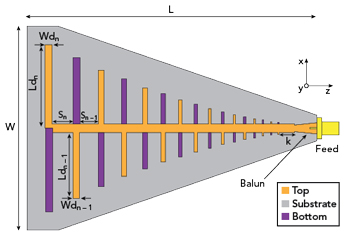
Figure 1 Antenna geometry.
The structure is like a standard, wire LPDA and it uses a typical LPDA design strategy.15 The LPDA antenna is shown in Figure 1. It comprises a set of dipole elements alternately printed on both sides of a microstrip substrate that is fed with an SMA connector to match the 50 Ω input impedance.
The resonant frequency of each dipole element changes periodically in conjunction with a logarithmic function related to the dipole size. Given N dipole elements:
Ldn = Length of the dipole element dn
Wdn = Width of the dipole element dn
Sn = Inter-element spacing between two adjacent dipoles
WL = Width of the microstrip feed line
LL = Length of the microstrip feed line
K = Feed length
These geometrical parameters must be properly tuned to realize a working antenna.
For a given desired bandwidth, where fmin and fmax are lower and upper cutoff frequencies, the design starting point is the definition of the parameters α, τ and σ considering the empirical rules defined by Milligan.16
The aperture angle α is given by Equation 1:

The scaling factor, τ, which is the ratio between lengths of two consecutive dipoles, Ldn and Ldn-1, is the most important design parameter. This relationship is shown in Equation 2:

The spacing constant σ is given by Equation 3:

The desired operating frequency range with upper and lower truncation constants, t1 and t2, determined for τ and σ are combined to compute the length of the longest element and determine the number of elements required. The longest element length is given by Equation 4:

where λ1 is the longest operating wavelength and t1 is determined empirically from Equation 5:16

The upper truncation t2 constant is defined as shown in Equation 6:

The truncation constants and the frequency band determine N as shown in Equation 7:

To determine the widths of the dipole elements and the feed line, the first assumption is that the required input impedance is real. The average characteristic impedance Z0 of the cylindrical dipole is given in Equation 8:17

where an = radius of the equivalent cylindrical dipole.
The width of the longest printed microstrip dipole element is approximatively equal to the perimeters of the cylindrical dipole as determined by Equation 9:3

After determining the length and width of the largest dipole element from Equation 4 and Equation 9, the lengths and widths of the remaining dipoles Wdn and Ldn for n = 1, 2, 3…N-1 are calculated by iterating the scaling factor τ.
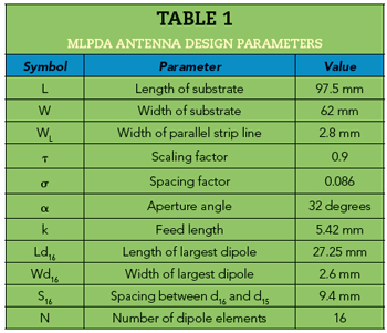
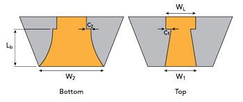
Figure 2 Balun geometry.
The prototype is fabricated on low-cost FR4 with a thickness of 1.5 mm, a loss tangent of 0.02 and a dielectric constant of 4.3. To cover the 2 to 18 GHz frequency range, N is determined to be 16, with τ = 0.9 and α = 32 degrees. The dimensions are optimized using CST Microwave Studio software. The design parameters used for analysis are listed in Table 1.
BALUN DESIGN
The operating band of a conventional LPDA may be arbitrarily widened by properly extending the geometry of the antenna structure and increasing the number of dipole elements.15 However, to practically achieve very large bandwidths, a balanced feed is required. From the simulation results, the antenna input impedance changes significantly as a function of frequency from 2 to 18 GHz. Hence, a balun is used to provide impedance matching.
This balun serves as a broadband impedance transformer to maximize power transfer. A balun based on the Klopfenstein microstrip tapered line is designed18 with the results shown in Figure 2. The balun contains two tapered lines printed on both sides of the substrate. The bottom and top lines combine to form a microstrip line at the unbalanced input of the balun. At the balanced output, both conductors are connected to one part of the antenna, constituting a balanced parallel strip. The impedance of the parallel strip is equal to the antenna input impedance. Along the balun, the top side includes a linearly tapered impedance transformer while the bottom side is an exponentially tapered microstrip. The exponentially tapered curve is described by Equation 10 with s and r defined through CST parametric optimization:

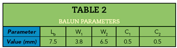
The antenna input impedance is approximately 166 Ω; therefore, the balun is designed to transform the unbalanced 50 Ω microstrip line to the antenna’s 166 Ω balanced impedance. The balun’s profile is optimized for minimum return loss, maximum bandwidth and reduced size. The balun dimensions are listed in Table 2.
RESULTS AND DISCUSSION
An antenna with and without the balun feed is designed and simulated using CST Microwave Studio. Their reflection coefficients are compared over frequency in Figure 3. They are similar below 8 GHz, but |S11| without the balun increases considerably beyond 10 GHz. The antenna with the balun exhibits an |S11| less than - 10 dB over a fractional bandwidth of 160 percent centered at 10 GHz.
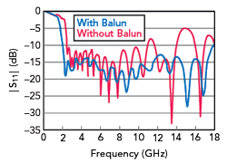
Figure 3 MLPDA antenna simulated reflection coefficient with and without a balun.
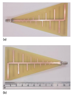
Figure 4 MLPDA prototype antenna: top view (a) and bottom view (b).
Figure 4a shows the top view of the prototype MLPDA antenna and Figure 4b shows the bottom view. A Keysight N5224A vector network analyzer is used to measure its electrical performance. Figure 5 shows the measured and simulated |S11| of the antenna, displaying good agreement between simulated and measured results. Small differences are attributed to tolerances in fabrication and assembly not accounted for in the ideal model.
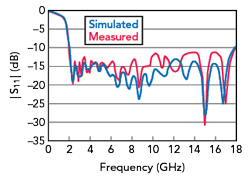
Figure 5 Simulated and measured MLPDA antenna reflection coefficient.
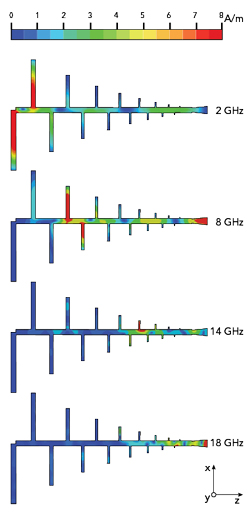
Figure 6 Simulated antenna surface current distribution at different frequencies.
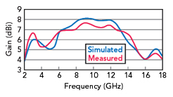
Figure 7 Simulated and measured antenna peak gain.
The surface current distribution is an efficient way to explain the antenna’s behavior. Figure 6 shows simulated current distributions on the antenna at 2, 8, 14 and 18 GHz. The active region moves toward the smaller dipoles when the operating frequency increases, as expected.
Antenna gain is also evaluated through measurement and simulation over the frequency band. The results are shown in Figure 7 and the simulated values are in close agreement with measurements. Peak gain is a maximum value of 8.16 dBi at 9 GHz and a minimum value of 3.9 dBi at 16 GHz.
Gain decreases at the operating bandwidth extremities. This can be explained by examining the radiation mechanism of the MLPDA. For a given resonating frequency, longer elements, as compared to those at resonance, act like reflectors while smaller arms act like directors. At the lowest frequencies, the gain degradation is due to the absence of a reflector behind the largest MLPDA element while the gain degradation at upper frequencies is attributed to the lack of directors before the shortest element.
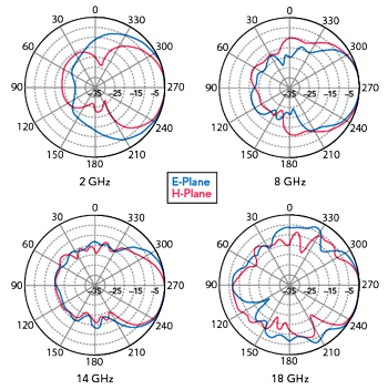
Figure 8 Radiation patterns at different frequencies.
Normalized radiation patterns for the broadband-fed MLPDA antenna are shown in Figure 8. They include end-fire radiation patterns at 2, 8, 14 and 18 GHz in the xz plane (E-plane) and the yz plane (H-plane). As mentioned previously, the pattern at 18 GHz becomes less directional in the absence of directors.
CONCLUSION
A wideband MLPDA antenna comprising 16 radiating elements and an integrated balun is printed on a low-cost substrate, which allows a simple realization and compact size. It demonstrates a 16 GHz impedance bandwidth and stable directional radiation patterns with an average gain of 6.2 dB. It is proposed for use in wideband portable devices operating in the 2 to 8 GHz range.
REFERENCES
- R. H. DuHamel and D. E. Isbell, “Broadband Logarithmically Periodic Antenna Structures,” IRE International Convention Record, March 1966.
- S. S. Pawar, M. Shandilya and V. Chaurasia, “Parametric Evaluation of Microstrip Log Periodic Dipole Array Antenna Using Transmission Line Equivalent Circuit,” Engineering Science and Technology, Vol. 20, No. 4, August 2017, pp. 1260–1274.
- C. K. Campbell, I. Traboulay, M. S. Suuthers and H. Kneve, “Design of a Stripline Log-Periodic Dipole Antenna,” IEEE Transactions on Antennas and Propagation, Vol. 25, No. 5, September 1977, pp. 718–721.
- S. Velicheti and P. Mallikarjuna Rao, “An Analytical Review on Log Periodic Dipole Antennas with Different Shapes of Dipole Elements,” Microelectronics, Electromagnetics and Telecommunications: Proceedings of the Fifth ICMEET, 2019, pp. 621–631.
- K. K. Mistry, P. I. Lazaridis, Z. D. Zaharis and T. H. Loh, “Design and Optimization of Compact Printed Log-Periodic Dipole Array Antennas with Extended Low-Frequency Response,” Electronics, Vol. 10, No. 17, August 2021.
- S. Yang, H. Zhai, J. Li and Y. Zeng, “A New Printed Log‐Periodic Dipole Array (PLPDA) Antenna with Bandwidth Broadening and Gain Improving,” International Journal of RF and Microwave Computer‐Aided Engineering, Vol. 30, No. 8, August 2020.
- Q. -X. Chu, X. -R. Li and M. Ye, “High-Gain Printed Log-Periodic Dipole Array Antenna with Parasitic Cell for 5G Communication,” IEEE Transactions on Antennas and Propagation, Vol. 65, No. 12, December 2017, pp. 6338–6344.
- Z. Yang, H. Jingjian, W. Weiwei and Y. Naichang, “A Printed LPDA Antenna Fed by a Microstrip Line to Double Sided Parallel Strip Line from Backside,” International Journal of Antennas and Propagation, Vol. 2017, October 2017.
- H. M. S. M. Herath, J. M. J. W. Jayasinghe and D. N. Uduwawala, “Performance Improvement of Printed Log Periodic Dipole Array Antennas,” IEEE 16th International Conference on Industrial and Information Systems, September 2021.
- H. Abutarboush, O. F. Siddiqui, M. R. Wali and F. A. Tahir, “A Highly Bendable Log-Periodic Array Antenna for Flexible Electronics,” Progress in Electromagnetics Research M, Vol. 96, September 2020, pp. 99–107.
- G. A. Casula, P. Maxia, G. Montisci, G. Mazzarella and F. Gaudiomonte, “A Printed LPDA Fed by a Coplanar Waveguide for Broadband Applications,” IEEE Antennas and Wireless Propagation Letters, Vol. 12, September 2013, pp. 1232–1235.
- G. Bozdag and A. Kustepeli, “Subsectional Tapered Fed Printed LPDA Antenna with a Feeding Point Patch,” IEEE Antennas and Wireless Propagation Letters, Vol. 15, June 2015, pp. 437–440.
- M. I. Mirzapour, S. M. J. Razavi and S. H. Mohseni Armaki, “Ultra‐Wideband Planar LPDA Antenna with Mode Converter Balun,” Electronics Letters, Vol. 50, No. 12, June 2014, pp. 848–850.
- F. Zengin, E. Akkaya, F. Günes¸ and F. N. Ecevit, “Printed Log‐Periodic Trapezoidal Dipole Array Antenna with a Balun‐Feed for Ultra‐Wideband Applications,” IET Microwaves, Antennas & Propagation, Vol. 12, No. 9, April 2018, pp. 1570–1574.
- R. Carrel, “The Design of Log-Periodic Dipole Antennas,” IRE International Convention Record, March 1966.
- T. A. Milligan, “Modern Antenna Design,” Second Edition, John Wiley & Sons Inc., IEEE Press, New Jersey, 2005.
- C. A. Balanis, Antenna Theory Analysis and Design, Third Edition, John Wiley & Sons Inc, New Jersey, 2005.
- R. W. Klopfenstein, “A Transmission Line Taper of Improved Design,” Proceedings of the RE, Vol. 44, January 1956, pp. 31–15.