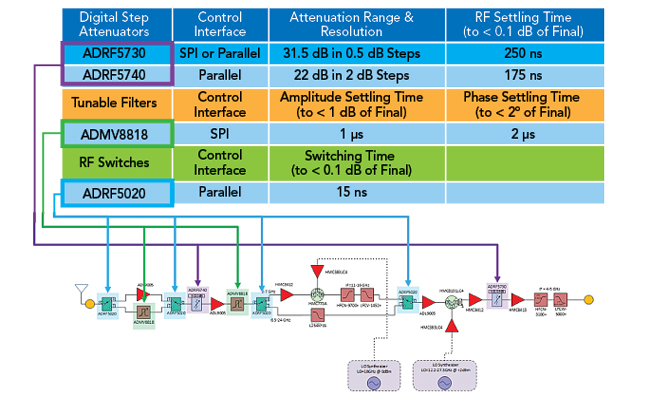
Nonlinear behavior modeling is essential in state-of-the-art RF front-ends, where digital timing and control knobs adjust performance while preparing signals for analog-to-digital conversion. The Analog Devices ADMV8818 tunable filter, for example, stores up to 128 states for its state machine overseeing preset filter configurations. Analog Devices had a concept for modeling their front-end reference design and sought Keysight’s help to construct a lookup table to coordinate states in PathWave System Design simulations. Figure 5 shows some of the variables in each state, including RF settling time. With these details added to the simulation, Analog Devices tuned digital settings and achieved a flatter frequency response across the 2 to 24 GHz operating range, matching physical measurements.

Figure 5 Controlling digitally-driven states accurately for RF front-end simulation (Courtesy of Analog Devices).
More nonlinear behavior is likely in store for 6G antennas. Achieving higher spectral density, which correlates to the number of bits that can be put in the air for a given channel, requires a combination of techniques. Advanced higher-order modulation packs bits of data more tightly into symbols, but these symbols are only valid if they arrive within acceptable error limits at the RF front-end.
6G researchers are looking at three technologies to break through channel interference and deliver more bits to more user equipment (UE), the devices in a 6G network, reliably. These three technologies are:
- Holographic beamforming that optimizes the shape of a beam using passive electronically steered arrays (PESAs) to increase the energy directed at a recipient with higher resolution compared to traditional phased arrays.
- Ultra-massive MIMO that utilizes thousands of antenna elements in coordination with beamforming to help improve the odds of signals overcoming significant sub-THz propagation loss and interference over greater distances.
- Reconfigurable intelligent surfaces (RIS) that incorporate reflective antenna elements in a programmable structure, possibly in 3D IC form. RIS aims to simplify designs by reducing the per-element RF signal chain processing requirements.
A mixed-signal context change is brewing overhead in non-terrestrial networks (NTNs). Bouncing signals off low earth orbit (LEO) satellites and other high altitude platforms injects a bulk delay due to extended distances and a Doppler shift resulting from satellite motion. Maintaining connections requires continuous pre-compensation for these effects at several points in the signal chain, including each UE.
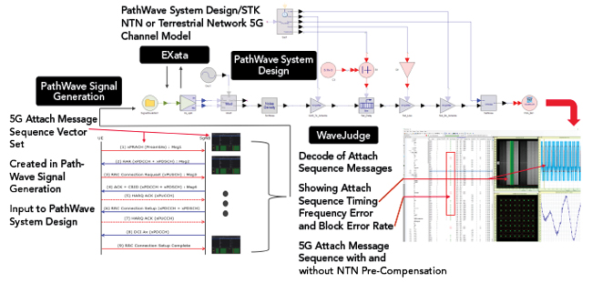
Addressing these challenges means system-level RF EDA tools must generate accurate 5G and, eventually, 6G messaging sequences and channel models for NTNs. End-to-end digital twins, enhanced with implementation measurement feedback, can help unlock suitable pre-compensation algorithms. Figure 6 illustrates initial research into this challenge, combining PathWave Signal Generation for creating authentic waveforms, EXata for core network timing simulation, PathWave System Design and Ansys STK for channel and kinematics modeling and WaveJudge for message decoding and timing analysis.

Figure 6 A conceptual model of a digital twin platform for NTN Doppler pre-compensation.
SUB-THZ CHALLENGES AND SCALABLE EDA WORKFLOWS
So far, this discussion has focused on RF system-level simulation needs. 6G design will also need full-bandwidth, multi-domain, nonlinear simulation capabilities at the component and module levels. Consequently, RF EDA will transition from single-purpose, specialized tools sharing data sequentially to a more integrated, scalable suite of enterprise-class tools delivering a comprehensive design experience. Several factors will drive this shift and include:
- New semiconductor and material technologies will call for new RF design architectures.
- Shorter wavelengths and wider bandwidths will expose effects hidden at lower frequencies.
- Substantially increased packaging and integration density will concentrate problem spaces.
- Manufacturability will become a significant challenge at higher frequencies and integration levels.
Advanced III-V semiconductor materials are seeing adoption in RF and power electronics. While these materials and processes offer new possibilities, system-level challenges such as higher noise floors and lower output power levels will intensify. High peak-to-average power ratio (PAPR) signals squeeze into narrower operating windows at mmWave frequencies with further dynamic range degradation at sub-THz frequencies.
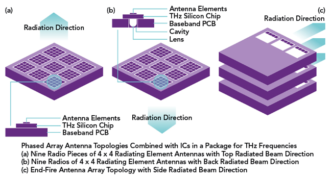
Another challenge involves effects stemming from the relative size of the signal wavelengths compared to the devices, packaging and their interconnects. mmWave frequencies push designs into a 3D guided-wave regime, introducing additional modeling complexity due to currents and components interacting in ways that can be ignored at lower frequencies. An example of this is new challenges presented by 3D current flow and ground references. Loss formulations, coupling, resonances and transmission modes all change, altering how ports must be set up, how ground references are made and how structures are designed to suppress unwanted interactions. In a 3D-stacked environment, power and ground distribution are linked to signal integrity and stability issues. Guided-wave port and excitation types require new calibrations, as do measurement and probing techniques and enclosures. Antenna elements can be directly designed into packaging like the monolithic mmWave IC concepts in Figure 7. While this reduces the number of components and size, weight and power (SWaP), care must also be taken to prevent crosstalk, signal contamination, EMI/EMC and even security risks.

Figure 7 Top-fire, bottom-fire and end-fire 3D IC antenna array concepts (Courtesy of 6G Flagship/University of Oulu).
Another shift is the trend toward greater package and integration density. Silicon devices will be complemented with RF front-end modules in other technologies and integrated into heterogeneous packages. This modular approach improves yields, lowers fabrication costs and mitigates technology risks but it increases process and tool complexity, along with interconnect, density and system challenges.
Process design kits (PDKs) will play critical roles in overcoming these obstacles. Design tasks become more complex when components from different processes and vendors integrate into one module, requiring co-validation for EM, thermal, stability and wideband modulated performance. Designs and PDKs must interoperate to address multiple effective stack-ups and dimensions within a single package.
Lastly, mmWave and sub-THz performance can vary significantly due to the tight tolerances associated with smaller wavelengths and material properties. ICs and packages become more sensitive to mechanical and material repeatability and thermal/environmental cycling. Measurement cabling, fixturing, probes and calibration standards also are vulnerable to these mechanical errors, leading to uncertainties. These complex environments have long, expensive fabrication timeframes and the modeling, validation and troubleshooting processes require more sophisticated skill levels and precise handling. All these factors increase design costs and hinder the pace of innovation. Monte Carlo simulation and design-for-manufacturing techniques can help, but some challenges are too difficult to address without computational assistance.
Scalable computation will be an essential element of next-generation EDA workflows. Cloud-based and high performance computing (HPC) platforms will become commonplace in many RF EDA workflows delivering simulation results with minimal wait times, keeping design team productivity high and shortening time-to-market. Digital twins with measurement-based simulation enhancements will represent complex RF components and subsystems before fabrication, enabling in-context RF system-level testing and troubleshooting impractical to execute in the real world.
AMPLE ROOM FOR AI TO HELP COMPLETE THE 6G DESIGN PICTURE
The complexity of the mmWave RF workflow is becoming unwieldy, necessitating a comprehensive digital transformation across the RF EDA workflow to prepare for the sub-THz era. EDA vendors and foundries are already striving for improved interoperability. A recent example of this trend is the innovation of an RFPro 3D EM-Circuit cockpit that interoperates between Cadence Virtuoso, Synopsys Custom Compiler, Keysight ADS and the just-approved 79 GHz TSMC 16 nm reference flow.
Managing models, scenarios, simulation data and result-driven optimization becomes a priority. AI techniques will take center stage and be applied in many ways. At the component level, AI will play a significant role in rapid model creation from datasheets or test data. This capability may manifest itself by scanning in a frequency response curve and automatically extracting S-parameters. Channel estimation and waveform design for 6G are also areas where AI is being explored. Sifting through simulation data and identifying mismatches against measurement data is also a task well-suited for AI. Ultimately, real-time, end-to-end 6G network optimization in response to the number of connected users and their traffic patterns at any given moment may only be possible using AI. Humans may be unable to describe the complex optimization for energy usage, capacity, latency and other network metrics in quantitative algorithm form.
RF EDA will play a pivotal role in firming up 6G specifications, creating sub-THz components and delivering advanced test and measurement equipment that enables complete 6G system design. For more insight on 6G requirements and innovation progress see:
RF Enabling 6G: Opportunities and Challenges from Technology to Spectrum
6G Technology: Envision the Future of Wireless Communications
https://www.keysight.com/us/en/solutions/emerging-technologies/6g-technology.html

