

Figure 10 compares the HFSS simulated S-parameters of the SSP-DGS and ASSP-DGS. Three transmission zeros at fz1a, fz2a and fz3a appear on the |S21| plot of the ASSP-DGS.
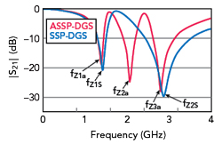
Figure 10 Simulated |S21| of SSP-DGS and ASSP-DGS compared (w1 = 1.5, g1 = 0.5, l1 = 5.5, a1 = 12, b1 = 13.8, sspla1 = 13.4, a2 = 11, b2 = 8.7, sspla2 = 8.3, sspwa = 0.25 and sspga = 0.4 mm).
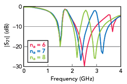
Figure 11 Simulated |S21| of ASSP-DGSs with different periodic number na (w1 = 1.5, g1 = 0.5, l1 = 5.5, a1 = 12, b1 = 13.8, sspla1 = 13.4, a2 = 11, b2 = 8.7, sspla2 = 8.3, sspwa = 0.25 and sspga = 0.4 mm).
Figures 11 and 12 compare simulated transmission responses of the ASPP-DGS with different periodic numbers na and groove depths sspla. The location of the transmission zero fz1a is insensitive to the change of the smaller defect structure. The zeros at fz2a and fz3a, however, are both drawn lower in frequency when either na or sspla is increased.
An ASSP-DGS with triple-band rejection is constructed by first defining the transmission zero frequencies fz1, fz2 and fz3 as well as the required rejection. A DB-DGS is designed with a transmission zero at around fz2. Then, an SSP-DGS with two transmission zeros fz1s and fz2s is designed with its loading parameters adjusted to make fz1s ≈ fz1 and fz2s > fz3. Finally, the ASSP-DGS is designed, based on the SSP-DGS, with three transmission zeros fz1a, fz2a and fz3a by adjusting the asymmetric defect structure to make fz1a ≈ fz1, fz2a ≈ fz2 and fz3a ≈ fz3.
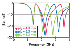
Figure 12 Simulated |S21| of ASSP-DGSs with different groove depth asspls (w1 = 1.5, g1 = 0.5, l1 = 5.5, a1 = 12, b1 = 13.8, sspla1 = 13.4, a2 = 11, b2 = 8.7, sspla2 = 8.3, sspwa = 0.25 and sspga = 0.4 mm). na = 8.
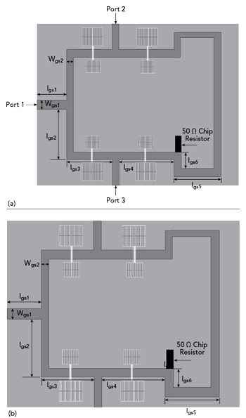
Figure 13 Gysel power divider layout with harmonic suppression: top view (a), bottom view (b).
POWER DIVIDER DESIGN
The power divider (PD) is a device that can divide an RF input signal into two or more output signals. Because it satisfies the reciprocity theorem, it can be used as a combiner as well. PDs are widely used as components in many microwave devices such as mixers, power amplifiers and antenna arrays. In these applications, unwanted harmonics caused by nonlinear circuit properties must be suppressed. A DGS can be incorporated as a harmonic rejection filter. The ASSP-DGSs are used to suppress the second, third and fourth harmonics.
The Gysel PD design with ASSP-DGSs is shown in Figure 13. The fabricated divider is shown in Figure 14. It is constructed on a 0.8 mm thick FR4 substrate with a relative dielectric constant εr of 4.4. The dimensions are:
wgs1 = 1.9, wgs2 = 1.7, lgs1 = 10, lgs2 = 22, lgs3 = 18.5, lgs4 = 43.5, lgs5 = 15, lgs6 = 16, g1 = 0.5,
l1 = 5.5, a1 = 12, b1 = 13.8, sspla1 = 13.4, a2 = 11, b2 = 8.7, sspla2 = 8.3, sspwa = 0.25 and sspga = 0.4 mm.
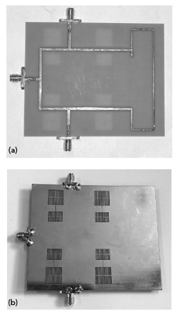
Figure 14 Fabricated Gysel power divider with harmonic suppression: top view (a), bottom view (b).
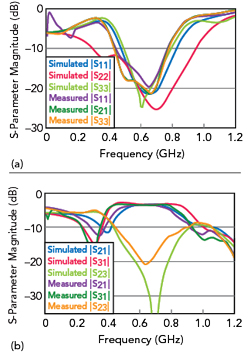
Figure 15 Simulated and measured S-parameters of Gysel power divider with harmonic suppression: |S11|, |S22|, |S33| (a) and |S21|, |S31|, |S23| (b).
MEASUREMENTS
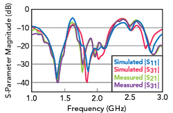
Figure 16 Simulated and measured |S21| and |S31| wideband performance of Gysel power divider with harmonic suppression.
Figure 15 shows simulated and measured S-parameters of the fabricated harmonic suppression Gysel PD. The matching bandwidth (|S11|, |S22| and |S33| < -15 dB) around the center frequency of 0.7 GHz is 24.3, 35.7 and 37.1 percent, respectively. The port isolation bandwidth (|S23| <-15 dB) is 30.1 percent. Measured |S21| is -3.6 dB and |S31| is -3.4 dB at 0.7 GHz.
Simulated and measured wideband |S21| and |S31| are shown in Figure 16. The suppression bandwidth (|S11| and |S22| < -15 dB) at the second, third and fourth harmonics is 26.4, 23.8 and 12.5 percent, respectively.
CONCLUSION
The ASPP-DGS described exhibits a response with three transmission zeros. Three harmonics can be suppressed simultaneously by adjusting the sizes of the DB grounds and the sizes of the internally loaded SSP structures. Performance is verified with the integration of four ASSP-DGSs into a Gysel PD providing second, third and fourth harmonic suppression. Both simulations and the measurements show suppression of the second, third and fourth harmonics with little loss at the operating frequency.
References
- D. Ahn, J. -S. Park, C. -S. Kim, J. Kim, Y. Qian and T. Itoh, “A Design of the Low-Pass Filter Using the Novel Microstrip Defected Ground Structure,” IEEE Transactions on Microwave Theory and Techniques, Vol. 49, No. 1, January 2001, pp. 86–93.
- D. J. Woo and T. K. Lee, “Suppression of Harmonics in Wilkinson Power Divider Using Dual-Band Rejection by Asymmetric DGS,” IEEE Transactions on Microwave Theory and Techniques, Vol. 53, No. 6, June 2005, pp. 2,139-2,144.
- W. -T. Liu, C. -H. Tsai, T. -W. Han and T.-L. Wu, “An Embedded Common-Mode Suppression Filter for GHz Differential Signals Using Periodic Defected Ground Plane,” IEEE Microwave and Wireless Components Letters, Vol. 18, No. 4, April 2008, pp. 248–250.
- C. Caloz, H. Okabe, T. Iwai and T. Itoh, “A Simple and Accurate Model for Microstrip Structures with Slotted Ground Plane,” IEEE Microwave and Wireless Components Letters, Vol. 14, No. 4, April 2004, pp. 133–135.
- L. S. Wu, B. Xia and J. F. Mao, “A Half-Mode Substrate Integrated Waveguide Ring for Two-Way Power Divider of Balanced Circuit,” IEEE Microwave and Wireless Components Letters, Vol. 22, No. 7, July 2012, pp. 333–335.
- B. Xia, L. S. Wu and J. F. Mao, “A New Balanced-to-Balanced Power Divider/Combiner,” IEEE Transactions on Microwave Theory and Techniques, Vol. 60, No. 9, September 2012, pp. 2791–2798.
- W. J. Feng, C. Y. Zhao, W. Q. Che and Q. Xue, “Wideband Balanced Network with High Isolation Using Double-Sided Parallel-Strip Line,” IEEE Transactions on Microwave Theory and Techniques, Vol. 63, No. 12, December 2015, pp. 4113–4118.
- J. Shi, J. Wang, K. Xu, J. X. Chen and W. Liu, “A Balanced-to-Balanced Power Divider with Wide Bandwidth,” IEEE Microwave and Wireless Components Letters, Vol. 25, No. 9, September 2015, pp. 573–575.
- H. T. Duong, H. V. Le, A. T. Huynh, N. Tran and E. Skafidas, “Design of a Compact Ultra Wideband Balanced-to-Balanced Power Divider/Combiner,” Proceedings of the Asia-Pacific Microwave Conference, November 2013, pp. 363–365.