

Figure 1 SSP-DGS.
Asymmetric spoof surface plasmon-defected ground structures (ASSP-DGSs) are developed from conventional dumbbell-shaped DGSs (DB-DGSs). By loading comb-shaped periodic SSP structures in the two rectangular defected areas and reducing the size of one side, the ASSP-DGS can produce three transmission zeros. Moreover, by changing the loaded SSP structure, the transmission zeros can be easily adjusted to obtain the desired rejection. The ASSP-DGS is incorporated in a Gysel power divider with triple-band rejection. Suppression bandwidths (|S21| < -15 dB and |S31| < -15 dB) at the second, third and fourth harmonics are 26.4, 23.8 and 12.5 percent, respectively.
In many modern wireless communication systems RF front-ends, harmonic rejection is important because harmonics interfere with desired signals. Various structures and techniques have been proposed to suppress them.1-9 Lowpass or bandstop filters can be used in many designs;1-3 however, both size and insertion loss often increase. Different filter structures with improved harmonic rejection have been proposed at the cost of increased design complexity and insertion loss.4-6
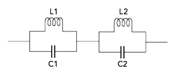
Figure 2 SSP-DGS equivalent circuit.
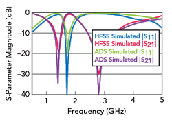
Figure 3 HFSS and ADS simulations.
DGSs are employed to suppress harmonics as well.7-9 Because DGSs can provide only one or two transmission zeros, multiple cascaded DGSs of different sizes must be employed to obtain rejection at several frequencies. The cascaded DGS configuration, however, increases insertion loss and circuit size.
In this work, a DGS with three transmission zeros is developed by combining a dumbbell-shaped DGS and SSP structures. HFSS and ADS simulations as well as parametric analyses are provided. It is found that the new DGS exhibits a response with three transmission zeros, rejecting multiple harmonics simultaneously. A Gysel power divider with triple harmonic rejection is designed. Experimental results agree closely with the simulation.
DGS WITH MULTIPLE TRANSMISSION ZEROS
SSP-DGS with Two Transmission Zeros
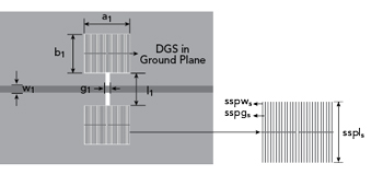
A DGS with two attenuation poles is first developed (see Figure 1). The SSP-DGS is created by loading comb-shape periodic SSP structures within the two rectangular defected areas of a conventional DB-DGS. The SSP groove depth and strip width are sspls and sspws, respectively, and the spacing between two adjacent strips is sspgs. The number of periodic unit cells is ns . The substrate is 0.8 mm thick with εr = 4.4.
The equivalent circuit of Figure 1 is analyzed, and the circuit parameters are extracted. A conventional DGS is equivalent to a single parallel LC circuit that blocks the signal at resonance. The SSP-DGS in this work is equivalent to two LC circuits in series (see Figure 2). Figure 3 shows simulation results of the SSP-DGS in both HFSS and ADS, demonstrating close agreement over a wide frequency range.
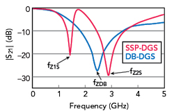
Figure 4 Simulated DB-DGS and SSP-DGS |S21| (w1 = 1.5, g1 = 0.5, l1 = 5.5, a1 = b1 = 12, sspls =11.6, sspws = 0.25 and sspgs = 0.2 mm).
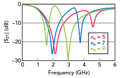
Figure 5 Simulated |S21| of SSP-DGSs with different periodic number ns (w1 = 1.5, g1 = 0.5, l1 = 5.5, a1 = b1 = 12, sspls = 11.6, sspws = 0.25 and sspgs = 0.2 mm).
Figure 4 compares the HFSS simulated |S21| of the conventional DB-DGS and the SSP-DGS. When the SSP structure is introduced, two transmission zeros at fz1s and fz2s appear on the |S21| plot. The location of the zeros can be adjusted by changing the loading of the SSP structure. As shown in Figure 5, when ns increases, the upper and lower frequency transmission zeros are both drawn lower in frequency. Similarly, as shown in Figure 6, the transmission zeros can be adjusted with different groove depths.
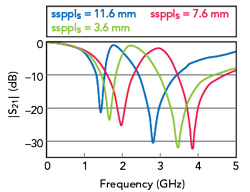
Figure 6 Simulated |S21| of SSP-DGSs with different groove depth sspls (w1 = 1.5, g1 = 0.5, l1 = 5.5, a1 = b1 = 12, sspws = 0.25 and sspgs = 0.2 mm). ns = 13.
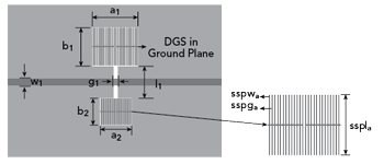
Figure 7 ASSP-DGS.
ASSP-DGS with Three Transmission Zeros
As shown in Figure 7, an ASSP-DGS is developed from a symmetrical SSP-DGS by reducing the size of the defect structure on one side. The ASSP-DGS is equivalent to three shunt LC resonant circuits in series as shown in Figure 8. Figure 9 shows simulation results of the ASSP-DGS in HFSS and ADS, demonstrating close agreement over a wide frequency range.
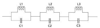
Figure 8 ASSP-DGS equivalent circuit.
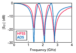
Figure 9 HFSS and ADS simulations.