Figure 1 The component side of a planar phased array front-end prototyping board.

Figure 2 A layout of one X-Band cell (top layer only).

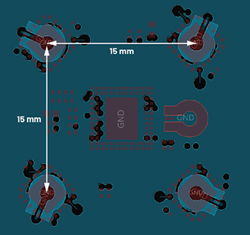
Figure 3 Top and bottom layers showing locations of SMPM connectors (Layer 1 pins superimposed for reference).
This article details the design and layout challenges associated with the electronic design of planar phased arrays and focuses on an RF front-end containing power amplifiers (PAs), low noise amplifiers (LNAs) and beamformers. The printed circuit board (PCB) layout discussion highlights a single cell, consisting of a beamformer surrounded by four transmit/receive (Tx/Rx) modules. Thermal management challenges are discussed, including component side heat sinking and heat sink cavity design with RF absorbers to avoid oscillations.
Two-dimensional planar phased array systems, where the RF circuitry and the antennal elements are on the opposite sides of the same PCB as shown in Figure 1, offer a significant size advantage over 3D blade-style structures. But that size advantage brings layout, power management and thermal challenges. This article will explore how some of these challenges can be dealt with using well-planned device functionality and interfacing, careful PCB layout that maximizes the usage of the limited available space and novel heat sinking techniques.
Phased array radar systems consist of many sections. These include the software and FPGA, ADCs and DACs, up-/down-converters, RF and beamforming circuitry and the phased array antenna elements. This article concentrates on the RF front-end and beamforming. In modern radars, the variable phase and amplitude blocks are consolidated into a beamformer integrated circuit (BFIC), with each BFIC containing several variable amplitude and phase blocks. Also, the PA, LNA and Tx/Rx switch can be integrated into a single Tx/Rx module and be optimally designed to work directly with the BFIC.
PCB LAYOUT
Phased array radar systems can vary in element count and size, from a 2 × 2 prototyping subarray to arrays that have 256, 512 or even 1024 elements. The array layout can be simplified down to a unit cell, typically connected to four elements. The cell size primarily depends on the lattice spacing, usually one half-wavelength (λ/2) so that no grating lobes appear for beam steering to the aperture horizon. Sometimes lattice spacing slightly greater than λ/2 is chosen for larger antenna gain and thinner beamwidths, this reduces the beam steering range without grating lobes. The location of the BFIC and Tx/Rx modules is usually constrained within the lattice spacing.
Cell Layout
An example cell layout on an Analog Devices planar phased array system board is shown in Figure 2. It features a four-channel BFIC with four Tx/Rx modules surrounding the BFIC. The layout goals of the cell were to make the lattice spacing 15 mm (λ/2 at 10 GHz) and length-match the RF Tx and Rx lines going from the BFIC to the four TR modules. The 10 GHz frequency was chosen for λ/2 as it is at the center of X-Band, where many radar systems are operated, along with some satellite communications systems. Length matching of the Tx and Rx interconnect lines between the BFIC and the Tx/Rx module reduces the burden on calibration.
The glueless interface between the BFIC and the four Tx/Rx modules results in almost no external components on the Tx, Rx or coupler lines going to the power detectors. This makes the layout routing efficient, which is shown in Figure 2. The glueless interface, along with the Tx/Rx module chips orientated at 45 degrees off-axis relative to the BFIC, easily enables the length-matched routing of the Tx and Rx lines, while also maintaining the 15 mm lattice spacing. Figure 3 shows the other side of the PCB, which contains RF connectors at 15 mm lattice spacing. In a real-world planar system, these connectors would be replaced with patch antennas.
Supply decoupling capacitors are kept at a minimum on this cell layout. The majority of the supply decoupling is for the BFIC. The Tx/Rx modules also have supply decoupling on the board, but most of these capacitors are technically not needed due to internal supply decoupling. Additional capacitors on the board were a conservative design decision and the 15 mm lattice spacing provided enough board space for these capacitors.

