

Overcoming Planar Phased Array Circuit Design Challenges

Figure 1 The component side of a planar phased array front-end prototyping board.

Figure 2 A layout of one X-Band cell (top layer only).
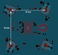
Figure 3 Top and bottom layers showing locations of SMPM connectors (Layer 1 pins superimposed for reference).
This article details the design and layout challenges associated with the electronic design of planar phased arrays and focuses on an RF front-end containing power amplifiers (PAs), low noise amplifiers (LNAs) and beamformers. The printed circuit board (PCB) layout discussion highlights a single cell, consisting of a beamformer surrounded by four transmit/receive (Tx/Rx) modules. Thermal management challenges are discussed, including component side heat sinking and heat sink cavity design with RF absorbers to avoid oscillations.
Two-dimensional planar phased array systems, where the RF circuitry and the antennal elements are on the opposite sides of the same PCB as shown in Figure 1, offer a significant size advantage over 3D blade-style structures. But that size advantage brings layout, power management and thermal challenges. This article will explore how some of these challenges can be dealt with using well-planned device functionality and interfacing, careful PCB layout that maximizes the usage of the limited available space and novel heat sinking techniques.
Phased array radar systems consist of many sections. These include the software and FPGA, ADCs and DACs, up-/down-converters, RF and beamforming circuitry and the phased array antenna elements. This article concentrates on the RF front-end and beamforming. In modern radars, the variable phase and amplitude blocks are consolidated into a beamformer integrated circuit (BFIC), with each BFIC containing several variable amplitude and phase blocks. Also, the PA, LNA and Tx/Rx switch can be integrated into a single Tx/Rx module and be optimally designed to work directly with the BFIC.
PCB LAYOUT
Phased array radar systems can vary in element count and size, from a 2 × 2 prototyping subarray to arrays that have 256, 512 or even 1024 elements. The array layout can be simplified down to a unit cell, typically connected to four elements. The cell size primarily depends on the lattice spacing, usually one half-wavelength (λ/2) so that no grating lobes appear for beam steering to the aperture horizon. Sometimes lattice spacing slightly greater than λ/2 is chosen for larger antenna gain and thinner beamwidths, this reduces the beam steering range without grating lobes. The location of the BFIC and Tx/Rx modules is usually constrained within the lattice spacing.
Cell Layout
An example cell layout on an Analog Devices planar phased array system board is shown in Figure 2. It features a four-channel BFIC with four Tx/Rx modules surrounding the BFIC. The layout goals of the cell were to make the lattice spacing 15 mm (λ/2 at 10 GHz) and length-match the RF Tx and Rx lines going from the BFIC to the four TR modules. The 10 GHz frequency was chosen for λ/2 as it is at the center of X-Band, where many radar systems are operated, along with some satellite communications systems. Length matching of the Tx and Rx interconnect lines between the BFIC and the Tx/Rx module reduces the burden on calibration.
The glueless interface between the BFIC and the four Tx/Rx modules results in almost no external components on the Tx, Rx or coupler lines going to the power detectors. This makes the layout routing efficient, which is shown in Figure 2. The glueless interface, along with the Tx/Rx module chips orientated at 45 degrees off-axis relative to the BFIC, easily enables the length-matched routing of the Tx and Rx lines, while also maintaining the 15 mm lattice spacing. Figure 3 shows the other side of the PCB, which contains RF connectors at 15 mm lattice spacing. In a real-world planar system, these connectors would be replaced with patch antennas.
Supply decoupling capacitors are kept at a minimum on this cell layout. The majority of the supply decoupling is for the BFIC. The Tx/Rx modules also have supply decoupling on the board, but most of these capacitors are technically not needed due to internal supply decoupling. Additional capacitors on the board were a conservative design decision and the 15 mm lattice spacing provided enough board space for these capacitors.
Another important goal of the cell layout was to keep the switching transients on the bias lines to a minimum so that switching times could also be minimized. This was accomplished by keeping the length of these lines as short as possible to reduce line parasitics. With the RF lines and supply decoupling on the top layer, the PA bias and LNA bias lines from the BFIC to the Tx/Rx module had to be routed on the PCB inner layers 4 and 5. The various digital control lines to the BFIC from the microcontroller were routed on Layer 5, which is shown in Figure 4 and Figure 5. On larger arrays with necessarily longer trace runs between the controller and BFICs and/or higher clock speeds, signal integrity simulations must be done to account for all trace propagation delays and ensure all digital timing is correctly synchronized.

Figure 4 Layer 4: PA bias, LNA bias and TR switch control routing (Layer 1 pins superimposed for reference).

Figure 5 Layer 5: LNA bias, TR switch control and digital routing (Layer 1 pins superimposed for reference).
On the Analog Devices planar phased array system board, the RFIO trace is short and immediately goes to a connector; thus, its isolation to other ports is high. However, on a real-world planar phased array application board, care must be taken when routing the Tx/Rx module antenna ports and the RFIO port, particularly the Channel 2 antenna and Channel 3 antenna ports shown in Figure 2 as they are on the same side of the cell layout as the RFIO port. While in transmit mode, the paths have higher gain relative to Rx mode and the isolation requirement between the paths is higher to prevent instability and oscillations.
THERMAL MANAGEMENT
In a planar phased array system with the antenna array on one side of the board and components on the other side, the heat sink must be located on the component side of the board. This presents a challenge for generating a thermal management solution that will effectively remove a sufficient amount of heat from the various components, particularly the PAs, so that none of the components exceeds its maximum junction temperature.
Options for Heat Management in a Planar Phased Array Antenna
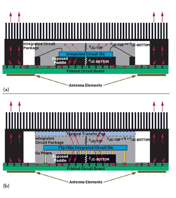
Figure 6 Component side heat-sinking with an LFCSP package with heat flowing primarily through the bottom of the package (a). Component side heat sinking with a copper-pillar flip-chip LGA package with heat flowing through the top and bottom of the package (b).

Figure 7 A planar phased array front-end with component side heat sink.
With the antenna array’s location on the back side of the board, the thermal management solution cannot rely solely on the heat being pulled from a component’s ground paddles through thermal vias to a back side-mounted heat sink. Instead, the heat must flow directly from the top side of the component or it must travel indirectly through the base of the component into the PCB, moving laterally before coming back out to a component side heat sink. This is shown in Figure 6a and Figure 6b. There are two possible options for heat conduction away from the components:
- The heat sink contacts large amounts of area of the top (component) side ground layer
- The heat sink contacts the top side of the components.
The heat sink design largely depends on the power dissipation and thermal resistance values of the components. Most components have a low junction-to-case bottom thermal resistance (θJC-BOTTOM) and relatively high junction-to-case top thermal resistance. So, the scheme shown in Figure 6a is generally more effective.
The question becomes whether to additionally contact the top side of the components or not. If the junction-to-case top thermal resistance (θJC-TOP) is of the same order of magnitude as θJC-BOTTOM (for example, θJC-TOP < 5 × θJC-BOTTOM) having the heat sink also contact the top side of the component packages would provide an additional useful parallel path for heat conduction. The metal of the heat sink should not contact the top of the package directly as this may cause mechanical stress. Instead, a piece of thermally conductive tape or a thermal transfer pad should be used as shown in Figure 6b.
A real-world example of component side heat sinking of a planar phased array is shown in Figure 7. This is the same planar phased array front-end board shown in Figure 1, only with the heat sink attached. Thermal conducting compound can be seen at the interface between the heat sink and exposed ground metal on the board (the white material along the edge of the heat sink). Also, note the absence of fins in strategic areas to allow access to the RF input/output ports of the ADAR1000 BFICs.
HEAT SINK CAVITY DESIGN
Component side heat sinking forces each cell of the four Tx/Rx modules and one beamformer to be inside a metal cavity. Care should be taken in the sizing and design of the cavity. An electromagnetic simulation should be performed to ensure that the cavity does not interact with the circuitry and result in instability or oscillations. Analysis of metallic cavities whether for shielding purposes or thermal management cannot be overlooked at high frequencies. Resonant modes are generally supported when the largest cavity dimension is greater than or equal to λ/2 of the operating frequency in free space. Energy radiated from circuitry and PCB traces within the cavity have nowhere to propagate beyond the confines of the cavity, possibly resulting in instability and oscillatory behavior of active circuitry.
Various techniques can be employed to mitigate the undesired effects of cavity mode resonances. These techniques can be as complex as custom metallic structures within the cavity that only support resonances at frequencies outside the range of operation. A much simpler technique is the placement of an RF-absorbing material within the cavity to attenuate the energy of the resonant modes. The absorber is composed of materials that create a high permittivity and high permeability of the electric and magnetic fields, respectively, for a range of operational frequencies. This is analogous to an electrical bandstop filter.
The mechanical dimensions of the cavities in the Analog Devices planar phased array system board heat sink do support resonances at frequencies within its operational range. To mitigate the effects of the resonant modes, a die-cut RF absorber is installed within each cavity to dampen resonances without degrading the performance of the board. The RF absorber attenuation ranges from approximately 20 to 50 dB/cm over the frequency band of operation, effectively lowering the Q-factor of the cavity resonator.

Figure 8 Gain measurements before and after installing the RF absorber.
An electromagnetic simulation of the heat sink cavity and RF absorber was performed using Keysight’s EMPro simulation tool. A simple model was constructed to analyze a single cavity representing the mechanical design of the heat sink cavity, the PCB material and a bulk material to emulate the ICs attached to the PCB. Two simulations were performed using the finite element method simulation engine to calculate the eigenmode resonances within the cavity. The cavity material for the first simulation was defined as air and resulted in eigenmode resonances with high Q-factors. In the second simulation, RF absorber material was used as the cavity material instead of air and this resulted in no eigenmodes. The second simulation case concluded the selected absorber material lowered the Q-factor of the cavity suppressing the resonant energy within the cavity. To ensure accuracy, the two simulation cases were verified with measured data from the hardware. The frequencies that support resonant modes as well as the reduction of the Q-factor by the RF absorber can be observed in the two gain measurements shown in Figure 8. These before and after measurements confirm the simulated predictions and highlight the importance of electromagnetic analysis.
CONCLUSION
In this article, we have looked at the challenges associated with designing the RF front-end of a planar phased array system. The size restrictions that stem from the required lattice spacing at high frequencies demand novel approaches to circuit design. These challenges can be significantly reduced through the use of BFICs and Tx/Rx modules, which easily interface together. This glueless interface has the additional benefit of shorter RF traces and fewer control lines, resulting in systems with fast responses that are easier to calibrate. Because one side of the PCB is reserved for the patch antenna array, compromises must be made to implement an effective heat sink. Proper heat sink cavity analysis and design are also vital to avoid oscillations.