We also adopted a slot to ground, common to all the resonators, rather than individual vias for grounding (see Figure 8), which adds additional flexibility and simplicity. With this topology, if the resonator lengths shift due to tolerances at least they all shift together. The center frequency may shift but the passband tuning is hardly affected.
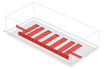
Figure 8 X-Band microstrip combline filter with N = 7, modeled with Sonnet. The via to ground is realized as a metalized slot in the substrate.
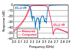
Figure 9 Measured vs. computed responses of the microstrip interdigital filter.11
If we build a microstrip interdigital or combline filter in an open environment or in a waveguide below cutoff, a transmission zero appears in the upper stopband due to non-adjacent couplings between the resonators (see Figure 9). Using an approximate technique,12 we proved to ourselves that including couplings between next nearest neighbors was not enough. All the non-adjacent couplings had to be included to come close to measured results.
Later in the mid-1980s, as computer power improved, we had access to more sophisticated 2D cross-section quasi-TEM and Spectral Domain Method models for multiple coupled strips in multilayer dielectrics. The quasi-TEM models generated a capacitance and inductance matrix that could be easily converted into an admittance matrix in a circuit simulator. The Spectral Domain models included energy that went into longitudinal section electric and magnetic (LSE and LSM) modes which had no simple, unambiguous conversion into an admittance matrix. Measured versus modeled results using these 2D cross-section methods can be found in the work of Swanson and Hoeffer.13
In late 1989 and early 1990 when the first 3D full wave electromagnet (EM) simulators appeared, they initially could only produce individual discontinuity models that we used to augment our 2D cross-section solver solutions. As EM simulation software became more efficient and computer power continued to increase, we could finally model the complete filter in a 3D EM environment. Like the inline cavity combline, we noticed interesting interactions between the filter and the cutoff waveguide channel that enclosed it. The resonators in any distributed printed filter couple to evanescent modes in the channel, which must be accounted for in the simulation.
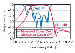
Figure 10 Measured interdigital filter, comparing the cover on and off.11
In Figure 10 we see measured results for the interdigital filter in Figure 7 with the cover on and off. The cover is far enough away from the substrate surface to preclude any significant influence on resonator impedances and coupling coefficients. Further proof is that when the cover is replaced by a coarse metal screen or even a metallic paper clip across the channel, the response returns almost exactly to the full cover case.
All this means we must choose the cross-section dimensions of the channel early in the design process. If those dimensions change, a redesign of the filter is often required. In the coupling matrix there is clearly no a priori method to include all the non-adjacent couplings found in microstrip combline and interdigital filters; therefore, it cannot predict the high side transmission zero that results from those couplings.
CROSS-COUPLED CAVITY COMBLINE FILTERS
Before we begin our analysis of specific filter examples, we need to review an important contribution to our understanding of how transmission zeros are realized in cross-coupled cavity combline filters. From Wenzel,14 three rules for how transmission zeros move in the com-plex plane are defined and two zero movement types are also defined (see Figure 11). In our filter examples we are primarily concerned with the behavior of a simple quad. To analyze the simple quad, we start with four inductively coupled resonators and add a capacitive cross-coupling from Resonator 1 to Resonator 4.
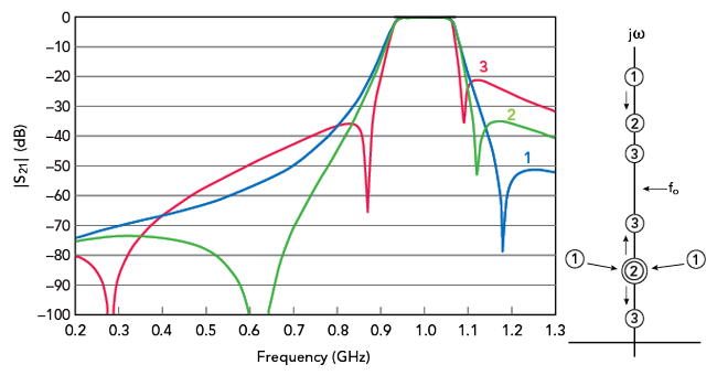
Figure 11 Movement of transmission zeros in the complex plane for a simple quad.14
Using the notation of Wenzel,14 as the capacitance is increased from zero, first a Type 1 zero appears above the passband and a complex quad of Type 2 zeros break off from infinity. As the capacitance increases further, two of the Type 2 zeros meet on the positive jω axis while the upper stopband zero moves closer to the passband. In the notation of Wenzel,14 this is the break frequency where the two low side zeros finally split and move in opposite directions.
We observe there are not one but two zeros in the lower stopband. Those zeros may be coincident, or not, depending on the filter bandwidth and tuning. In either case, the result is the asymmetric stopband rejection we will observe in our filter examples. It is this complex zero movement that cannot be reproduced by a coupling matrix. When we introduce a simple quad in conventional coupling matrix software, a single zero appears in the lower and upper stopbands and the two zeros move with almost perfect symmetry for any value of the capacitive cross-coupling.
FOLDED CROSS-COUPLED COMBLINE FILTER EXAMPLES
Our first example is a folded N = 6 combline filter from an excellent tutorial paper by Morten Hagensen15 that includes measured data (see Figure 12). This filter is located in the WiMax band and has 3 percent relative bandwidth, which is well within the acceptable range for the coupling matrix approach.
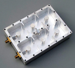
Figure 12 Folded N = 6 combline filter with two transmission zeros.15
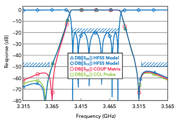
Figure 13 Simulations with the capacitive probe modeled as a transmission line cascade: HFSS (blue), coupling matrix (red) and CCL (green).
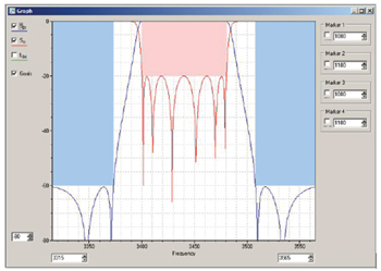
Figure 14 Coupling matrix prediction for two cross-couplings in the N = 6 folded filter. The stopband rejection stays symmetrical for all cross-coupling values.
We generated network theory and EM models to contrast with the coupling matrix prediction for this filter. If we place a capacitive (negative) coupling between Resonator 2 and Resonator 5, the coupling matrix predicts nearly perfect symmetry in the stopbands (see Figure 13). This symmetry is maintained as we increase or decrease the magnitude of the cross-coupling; but, the measured data, the network theory model and the 3D FEM model each present the asymmetric response predicted in the previous section.
After many years of experience with port tuning, we trust the 3D EM model to be correct. Even with a simple lumped capacitor cross-coupling in the network theory model we see the same type of asymmetry predicted by the EM model. As we increase the complexity of the capacitive probe model, correlation with the EM model gets better and better.
In his tutorial paper, Hagensen15 speculates that the asymmetry observed in the measured hardware is due to a parasitic coupling from Resonator 2 to Resonator 4; however, there are no parasitic couplings in our network theory model, which agrees with the 3D EM simulation.
A more dramatic example can be found when we add a second inductive (positive) cross-coupling from Resonator 1 to Resonator 6. Again, the coupling matrix tells us the rejection in the stopbands will be very symmetrical, no matter what magnitudes we choose for the two cross-couplings (see Figure 14).
