
This article describes the design of a bias tee for a pulsed-bias, pulsed-RF test system. The cut-off frequency of the DC path was raised to allow pulsing of the bias signal. The theory of bias tee design for pulsed measurements is first presented. The simulation results for the design without the use of component models are presented, followed by simulation results obtained using accurate parasitic models for the inductor and capacitor used. The simulation results are then compared with S-parameter measurements obtained using a TRL calibration and found to show good agreement. Finally, illustrations of the accurate use of the bias tees in performing both pulsed IV and pulsed S-parameter measurements are provided.
Bias Tee Design

A typical bias tee circuit consists of an inductor and a capacitor, as shown in Figure 1. The function of the bias tee is to simultaneously allow a DC bias voltage and an RF test signal to be applied to the port of a transistor during measurement. For example, in an S-parameter measurement system, the DC bias is applied at the port labeled “DC,” and the RF test signal from the vector network analyzer is applied to the port labeled “RF.” At the RF + DC port, both the RF and DC voltages are applied to the device. The purpose of the inductor is to prevent the RF signal from entering the DC path, and the purpose of the capacitor is to keep the DC signal from entering the RF path. The inductor and capacitor should be designed such that the upper cut-off frequency of the low pass DC path is lower than the lower cut-off frequency of the high pass RF path. If this is true, then the lower cut-off frequency of the RF path containing the capacitor (considering the inductor to be an open circuit) is given by

![]()
where R is the total resistance seen at the capacitor terminals. In this case, the termination at the RF port is 50 Ω and the termination at the RF + DC port is large (either the input or output impedance of the device) in normal operation but will be 50 Ω in the bias tee test setup. In operation, however, the value of the input resistance will be fairly large, changing the cut-off frequency. However, in a 50 Ω test system, 50 Ω is the impedance at all test ports. This setup will be used for the purpose of benchmarking the behavior of the device through measurement and simulation. Thus, R = 50 + 50 = 100 Ω for this case.

The cut-off frequency of the DC path, assuming that the capacitor appears as an open circuit, is given by
![]()
In this case, R is equal to the sum of the impedance presented by the bias equipment and the input impedance to the device under test. For a 50 Ω test system, R = 50 + 50 = 100 Ω.
The outstanding factor for a pulsed bias tee design is that the cut-off frequency of the DC path must be high enough to allow the pulsed bias signal to proceed unabated from the DC to the RF + DC ports. In this case, the smallest pulse length to be used for pulsing the bias is approximately 100 ns. The frequency content of this pulse is a (sin x)/x function centered at a frequency of 1/(100 × 10–9) = 10 MHz. Thus, the upper cut-off frequency of the bias network should be greater than 10 MHz, large enough that the entire frequency content of the pulse can pass through the DC path without distortion; this will allow the integrity of the pulse shape to be maintained.
Initial values for the inductor and capacitor were chosen and simulations containing ideal elements were performed to ensure the selection of component values that will provide adequate cut-off frequencies for the DC and RF paths. The simulations were performed using Agilent Technologies’ Advanced Design System (ADS). The simulation circuit and results for ideal component values of C = 100 pF and L = 27 nH are shown in Figures 2 and 3, respectively. For these component values, the 3 dB cut-off frequency of the RF path is shown to be 151 MHz and the cut-off frequency of the DC path is shown to be 61 MHz.
Simulation Results

Simulations were performed for the selected component values L = 27 nH and C = 100 pF. The simulation was performed at three different levels. At each level, both S-parameters and transient simulations were run. The purpose of the S-parameters simulation is to ensure that the RF path of the bias tee passes the signal while the DC path does not at RF frequencies. The transient simulation is used to show that the pulse can accurately reach the RF + DC port without being significantly distorted in the time domain. Three levels of simulation were incorporated into this effort: (1) ideal components and no transmission lines; (2) ideal components with microstrip (FR-4 substrate) transmission lines; and (3) lumped component parasitic models developed by Modelithics, combined with microstrip transmission line models built-in to Agilent ADS. The first level was used to assess the optimum inductance and capacitance values, as shown in the previous section; the second and third levels are used to view non-idealities introduced by the substrate (second level) and component parasitics (third level).

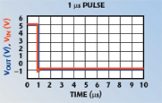
For the first-level schematic, the simulation results are displayed in Figures 4 and 5. They show that the S-parameter results are as desired. From approximately 500 MHz and above, S31 is high (which means that most of the input signal is getting to the RF + DC output) and S21 is low (very little signal is going from the RF port to the DC port). Also, S11 is below approximately –20 dB for all frequencies greater than approximately 1.7 GHz. These results show that the choice of component values seems reasonable for a large RF passband. The transient simulation reveals whether the bias tee will allow accurate transmission of pulses from the DC port to the RF + DC port. The results show that a 1 μs square pulse sent from the DC port appears virtually undistorted at the RF + DC port, and a 0.1 μs pulse also goes through the system with only minimal overshoot at the rising and falling edges of the pulse. Since 0.1 μs is short enough for isodynamic measurements, it appears that this bias tee is designed correctly with regard to the DC path passband.
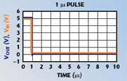
The next step was the incorporation of microstrip lines into the simulation. Ideal components, however, were still used for the inductor and capacitor, as shown in Figure 6. The substrate parameters used in the “MSUB” element are those for the FR-4 substrate to be used in milling the circuit. Figure 7 shows the S-parameters simulation results for the microstrip circuit. While the circuit behavior is still close to ideal up to approximately 5 GHz, there is a steep drop in S31 at approximately 8 GHz. In addition, the input match becomes worse as the frequency increases, reaching a peak at the same location as the notch in S31. However, these simulations indicate that the bias tee should be useful in applications up to 6 GHz. The transient simulations are shown in Figure 8. Excellent pulse integrity is obtained at the RF + DC port.
Finally, the simulations were performed using detailed models for the components to be used in the circuit: a TDK 27 nH size 0603 inductor and an ATC 100 pF size 0603 capacitor. The models include the bond pads, so these were not included in the microstrip components. However, it is necessary to include these bond pads in the schematic for the layout generation.

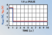
Figure 9 shows the schematic used for the simulation. Figure 10 displays the S-parameters simulation results. The plots show that the response concerning the RF to DC port and RF to RF + DC port transmissions is adequate at frequencies below 4 GHz. However, at 4.5 GHz, more transmission is occurring from the RF port to the DC port than from the RF port to the RF + DC port. In addition, the input match at this frequency is relatively poor, as evidenced in the S11 plot. These non-ideal effects are due to the component parasitics, since the microstrip line elements added in the second simulation stage did not cause such effects at these frequencies. They will limit the frequency range for which the bias tee will be able to be accurately used in S-parameter measurements. Figure 11 shows the transient simulation results for the bias tee. It appears that the height of the pulse at the RF + DC port is slightly lower than at the input. This is likely due to the non-ideal resistance of the components that is included in the models but is not taken into account in the ideal component definitions used for the simulations whose results were previously displayed. The use of three levels of simulation has shown that both the transmission line elements and the parasitic effects of the components have a substantial impact on the S-parameters simulation results. With the addition of the transmission line elements and component models, it was seen that some non-ideal effects are expected to occur above 4 GHz.

Layout and Fabrication
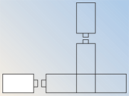
The bias tees were constructed by mounting the components on a 59-mil thick FR4 substrate. The circuit board was fabricated in the University of South Florida (USF) Wireless and Microwave Instructional (WAMI) Laboratory. The layout for milling was generated using a schematic in Advanced Design System with the components replaced by bond pads and a small gap. The bond pads were not part of the previous schematics used for simulation because the effects of the bond pads were included in the models for the simulations. The schematic used to generate the layout is shown in Figure 12 and the layout generated by ADS for milling is shown in Figure 13.
S-parameter Measurements of Bias Tees
To test the accuracy of the models in predicting the behavior of the bias tees, S-parameter measurements were performed over a frequency range of 40 MHz to 6 GHz using an Anritsu 37397C “Lightning” vector network analyzer. A through-reflect-line (TRL) calibration was used for the measurement. The 59-mil FR4 standards used for this calibration have coaxial-to-microstrip adapters at each port. The length of the standards was measured in the USF laboratory. The through standard was measured to be 10.00 mm, while the delay standard was measured as 18.64 mm. The open was offset by half of the through standard line length. The calibration was performed using the Multical Software created by the National Institute of Standards and Technology (NIST). A reference impedance of 50 Ω and an effective relative permittivity of 3.3 were used. The reference plane was set to be 5 mm from the center of the through, placing it at the beginning of the microstrip line, just on the microstrip side of the coaxial-to-microstrip adapter at each port. Figure 14 shows plots of S31, the RF to RF + DC transmission, in dB magnitude and phase. The largest difference between the results in both magnitude and phase occurs between 5 and 6 GHz.

The measured versus simulated (without microstrip-to-coaxial adapters) results for S21 (the RF to DC transmission) are shown in Figure 15. The magnitude of S21 should be low at all frequencies. A very good agreement is obtained between the measured and simulated data in both magnitude and phase. Measured and simulated results for S32 (DC to RF + DC transmission) are shown in Figure 16. The magnitude of this transmission is expected to be low except at low frequencies. The magnitude match is excellent between measured and simulated results over the entire measurement band for both S21 and S32.
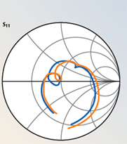
Figure 17 shows the measured and simulated input reflection coefficient results for all three ports. The simulation and measured reflection parameters match well at lower frequencies; however, some differences exist at higher frequencies. The simulated parameters have larger magnitude in each case at the higher frequencies, especially S33. This may be due to the difficulty of obtaining a good reflection calibration using a 59-mil FR4 substrate with SMA-to-microstrip adapters at higher frequencies. Figures 18, 19 and 20 display the reflection parameters as magnitude and phase versus frequency.
In general, the S-parameter results show good agreement from 40 MHz to 5 GHz. This data seems to indicate that the models have accurately predicted the performance of the design on the first pass.
Pulsed IV Measurement Through Bias Tees
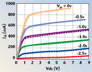
In addition to testing the RF performance of the bias tee, it is also important to ensure that the circuit allows a pulsed bias to be correctly applied to a device under test. A good test method for this is to attempt to perform pulsed IV measurements through the bias tees as attempted previously;1 if the bias tees do not distort the IV curves, they are adequate for applying a pulsed bias to an RF measurement system. In this experiment, pulsed IV measurements with pulse lengths varying from 0.1 to 1000 ms were performed on a GaAs MESFET, using an Accent Optical Technologies Dynamic i(V) Analyzer (DiVA) model D225. The measurements were performed for three setups: (1) no bias tees; (2) a set of commercially available bias tees; and (3) a set of USF custom bias tees. In the bias tee setups, the DiVA was connected to the DC ports of the bias tees and the RF ports of the bias tees were terminated in 50 Ω loads. The measurement setup is shown in Figure 21. For the commercially available bias tees, the measurements were performed for pulse lengths varying from 1000 to 5 μs. When attempting to measure at 2 μs, the instrument reported that it could not complete the measurement due to the large amount of gate current. Measurements were performed for the custom USF bias tees from 1000 to 0.1 μs. From simulation and initial transient measurement results, it was expected that the bias tee would function very well for pulse lengths as low as 0.1 μs. In addition, it is desired to perform pulsed IV measurements within the pulsed S-parameter system, so it is critical that the IV characteristics be accurately measurable through the bias tees. Figure 22 shows pulsed IV curves taken with different pulse lengths for the commercially available bias tees and the custom USF designed bias tees. In each plot, the dashed sets of curves are the measurements without bias tees. At 1000 μs, there is a “jog” in the knee region characteristic of the curves without bias tees. For measurements made with the commercial bias tees, this jog is not measured; however, the USF bias tees correctly depict this shift in the curves. The physical phenomenon behind this shift may be due to trapping effects. The commercial bias tees may lengthen the resetting time between pulses, so this effect is likely not due to the pulse length, but the pulse separation, as shown in Reference [3] for this device. If the pulse separation were lengthened, this result would likely to improve. However, even in this situation, it is interesting to note that the custom bias tees more closely represent the measurement environment where no bias tees are used.

The figure also shows that the commercially available bias tees cannot allow accurate pulsed IV measurement for pulse lengths below about 20 μs. Both bias tees allow accurate measurement of the 20 μs curves. At 10 μs, the IV curves measured through the commercial bias tees are too greatly sloped (gds is too large), while the custom bias tees allow accurate measurement of the curves. For a pulse length of 5 μs, the commercial bias tees are very clearly in error. The 0.1 μs pulse length measurement through the custom bias tees is compared to a 0.1 μs pulse length measurement without bias tees in Figure 23.
In the custom bias tee measurements, the knee appears to occur at a slightly larger value of VDS than for the measurements without bias tees. This is likely due to the fact that both the inductor and the coaxial-to-microstrip adapters, the FR4 substrate microstrip transmission lines, the solder joints and the inductors themselves add resistance to the drain side of the device, causing a lower voltage to be applied to the device than in the case where no bias tees are used. This DC resistive effect can be easily corrected using a Mathcad sheet if the resistance is measured. In addition, the figure shows that the curves measured through the bias tees are slightly higher than the curves measured without bias tees.

Pulsed S-parameters Measurement Results
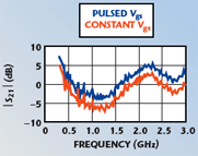
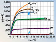
The pulsed bias tee has been used successfully in the design of a pulsed-RF, pulsed-bias S-parameter measurement system, as documented by a recent conference paper.4 Figure 24 shows the S21 measurement results for a 5 W Si laterally diffused MOSFET (LDMOSFET) under both pulsed- and continuous-bias measurement conditions. The RF signal is pulsed in both situations; however, the bias signal is pulsed in one case and is held continuous in the other case. As documented by Parker, et al., the difference in |S21| can be attributed to self-heating in the device.5 This can be predicted from the IV curves of the device, which are shown in Figure 25. The bias point A is the “pulse-from” bias, while the bias point B is the “pulse-to” bias, the bias at which the measurement is performed. For the gate-voltage, drain-voltage combination given by the bias point B, the difference between the current values is substantial. Notice also that the spacing between the surrounding curves is vastly different, which indicates a significant difference in the small-signal value for gm at this bias point between the pulsed- and continuous-bias cases. This manifests itself in a lower gain for the continuous-bias case, because the value of gm is lower. This is exactly what is observed in the previous figure.

Conclusion
A custom bias tee design has been obtained with the assistance of accurate passive component models to accommodate pulsed-bias, pulsed-RF S-parameters measurements with pulse lengths on the order of 1 μs and lower. The simulation results for the time and frequency domains are found to compare remarkably well with the use of the models. An incremental design procedure for this circuit has been demonstrated, followed by the results of measuring pulsed IV characteristics through the bias tees. The pulsed IV results for the custom bias tees are far more accurate than those performed through commercially available bias tees, which are not normally designed to allow pulses to pass through the bias path. Finally, initial pulsed-bias, pulsed-RF S-parameter measurement results are shown and found to correlate with expectations. The design of custom bias tees for pulsed applications using accurate component models has provided first-pass success with the construction of this pulsed measurement system.
References
1. C. Baylis and L. Dunleavy, “Understanding Pulsed IV Measurement Waveforms,” 2003 IEEE International Symposium on Electron Devices for Microwave and Optoelectronic Applications Digest, Orlando, FL.
2. C. Baylis, “Improved Current-voltage Methods for RF Transistor Characterization,” Master’s Thesis, University of South Florida, 2004.
3. C. Baylis, L. Dunleavy and A.D. Snider, “The Normalized Difference Unit as a Metric for Comparing IV Curves,” 64th Automatic RF Techniques Group Conference, Orlando, FL, December 2004.
4. C. Baylis, L. Dunleavy and J. Martens, “Constructing and Benchmarking a Pulsed-RF, Pulsed-bias S-parameter System,” 66th Automatic RF Techniques Group Conference, Washington, DC, December 2005.

5. A. Parker, J. Scott, J. Rathmell and M. Sayed, “Determining Timing for Isothermal Pulsed-bias S-parameter Measurements,” 1996 IEEE MTT-S International Microwave Symposium Digest, Vol. III, pp. 1707–1710.
Charles Baylis received his BS degree in electrical engineering and a minor in mathematics, summa cum laude, from the University of South Florida in 2002 and his MS degree in electrical engineering in 2004. He is now pursuing his PhD degree in the Center for Wireless and Microwave Information Systems at the University of South Florida. He serves as an adjunct instructor and a research assistant under the guidance of Lawrence Dunleavy, where he is focusing on the development and applications of pulsed measurement and electrothermal transistor characterization methods.
Lawrence P. Dunleavy received his BSEE degree from the Michigan Technological Institute in 1982 and his MSEE and PhD degrees from the University of Michigan in 1984 and 1988, respectively. He has worked in industry for E-Systems (1982–1983) and Hughes Aircraft Co. (1984–1990), and was a Howard Hughes doctoral fellow (1984–1988). In 1990, he joined the electrical engineering department at the University of South Florida, where he is now a professor and co-founder of the University’s Center for Wireless and Microwave Information Systems. In 2001, he co-founded Modelithics Inc. to provide practical commercial modeling solutions and microwave measurement services for RF and microwave designers.
William Clausen received his BSEE and MSEE degrees from the University of South Florida in 2003. He has been a member of the technical staff at Modelithics Inc. since 2002. His current interests include microwave measurements, active and passive component modeling, and amplifier design.



Charles Baylis

Lawrence P. Dunleavy

William Clausen
