

Abstract
This tutorial is a comparative study of two of the most common computational electromagnetics (CEM) solvers, FEM and MoM applied to a practical filter application. Both solvers are used to evaluate a 1 GHz, stepped-impedance, low-pass filter design. The filter design is described along with its ideal schematic results. A layout is generated and both electromagnetic solvers are applied. EM results of the two solvers are compared with the ideal schematic simulation and measurements. The CEM simulators reveal aspects missed by traditional schematic-based simulators. Insight into the differences between the two are discussed as well.
Introduction
CEM plays a critical role in modern electronic design and simulation, especially at microwave frequencies. General printed circuit board and integrated circuit design begins with schematic-based simulations and then moves to design layout. Once the layout is complete, electromagnetic (EM) simulators are used to provide the designer insight into how parasitics and EM/RF properties, such as coupling and the skin effect, may affect the design.
There are several CEM solvers available. Two of the most common are MoM and FEM.1 Both of these discretize geometries to numerically solve Maxwell’s equations for current densities. E- and H-fields can then be determined along with scattering parameters, Poynting vectors for EM power flow, wave dispersion and more. One major distinction between them is how they solve Maxwell’s equations. MoM uses integration methods while FEM uses partial differential equations. Each has its advantages and disadvantages, although both can be significantly accurate.
Background
Method of Moments
MoM is one of the most widely used CEM techniques in the high frequency world.1 In MoM, radiating and scattering structures are replaced by equivalent surface currents that become discretized in either wire segments or surface patches (also known as meshing). Once discretized, each cell’s current density is computed utilizing Green’s function. Green’s function uses integration techniques to compute closed-form solutions to uncoupled partial differential equations derived from Maxwell’s equations.2
This method uses a unit source, such as an impulse response, as the driving function. In system theory, Green’s function simply solves the impulse response, or transfer function, of each the segmented sections for its current density. This enables enhanced computational speed and increased efficiency.
It is worth noting that MoM and Green’s function solve only for the surface current density, while using approximations to account for equivalent substrate and volumetric currents. For this reason MoM is sometimes considered a 2.5D EM solver. Additionally, MoM computations are applied in the frequency domain, hence the working variables are complex, with both magnitude and phase components.1
The strength of MoM is its treatment of conductive surfaces. Since it performs only surface meshing, “air” and boundary meshing are eliminated. This increases overall efficiency while still providing high accuracy surface current modeling. Additionally, MoM automatically incorporates the far-field behavior from the source or “radiation condition,” which is particularly important when evaluating radiation or scattering parameters.1
An apparent weakness of MoM is that is cannot accurately handle pure three-dimensional structures where inhomogeneous materials are used. This is because MoM uses surface meshing, and to appropriately analyze inhomogeneous three-dimensional structures, volumetric meshing is required.
Furthermore, meshing frequency and run time do not increase together linearly. That is, as the frequency of operation, or meshing frequency, increases, the run time is scaled by the power of six. For example, if the meshing frequency doubles, the run time can be up to 64 times longer.1 This makes it more difficult to work with higher microwave frequency devices or applications that require finer meshing (i.e. a higher meshing frequency). Nonetheless, MoM is a powerful, efficient and potentially accurate solver for a majority of RF and microwave circuit applications.
Finite Element Method
FEM is another widely used and trusted electromagnetic solver. In contrast to MoM, FEM is a full 3D EM solver using both surface and volumetric meshing techniques, allowing it to better handle inhomogeneous materials. FEM, again, begins with the partial differential equation form of Maxwell’s equations. The material is then discretized into a finite element mesh composed of triangular and tetrahedral meshed sections. Typically, surfaces are meshed triangularly, while volumetric meshing employs tetrahedrons.
Similar to MoM, FEM generally computes current densities and E- and H- fields in the frequency domain, yielding complex magnitude and phase components. FEM solves Maxwell’s equations by using variational analysis. It finds a variational functional (i.e. functional derivative) whose extremal point corresponds with the solution of the partial differential equations, subject to boundary conditions;1 that is, it solves Maxwell’s equations using algebraic systems of equations until the weighted error function, sometimes called a delta error, is minimized.
In software such as Keysight’s Advanced Design System and EMPro, this delta error value is defined by the user and refers to the allowable change in magnitude of the vector differences for all computed S-Parameters.3 An initial finite element mesh is defined, EM fields are solved for, and then S-Parameters are computed. These EM fields and S-Parameters are then re-computed and compared with the former results. 9876If the magnitude of the complex S-Parameter vector difference between runs is greater than the specified delta error, a finer mesh is re-defined, and the process repeated until the delta error is satisfied.
The most significant strength of FEM is its straightforward treatment of complex 3D geometries and inhomogeneous materials by applying the triangular and tetrahedral finite element mesh technique.1 This allows it to accurately handle full 3D geometries. Additionally, it can solve source-free problems, such as waveguides or cavity resonators where there resides eigenmodes, resonant frequencies and associated fields distributed throughout the component. FEM also has a slightly better frequency scaling to run-time relationship compared to MoM, with run time scaled by a power of 5.5 as opposed to 6.
A weakness of FEM is its efficiency. Since full volumetric meshing is performed, computations are much more complex and their speeds are typically slower than for MoM. Additionally, FEM does not inherently include the far-field behavior, or radiation condition. For closed regions such as waveguides, however, this is irrelevant. For open regions, such as patch antennas, where radiation and scattering must be characterized, special consideration must be taken. Typically, this is done by including some arbitrary region between the radiator and absorber for the solver to mesh and solve.1
Although FEM may be more complex than MoM, it is powerful, making it one of the preferred methods for microwave device simulation.
Filter Design
The example used in this tutorial is a 1 GHz Chebyshev, seventh-order, stepped-impedance low-pass filter. It is designed to satisfy the performance specifications outlined in Table I. With a corner frequency of 1 GHz, high frequency RF and EM effects must be considered in the design layout.
Table I: Filter Design Specifications
Parameter |
Description |
Value |
Unit |
fc |
-3 dB corner frequency |
1.0 |
GHz |
As |
Min stop-band attenuation at fc + 200 MHz |
23.0 |
dB |
Ap |
Max passband insertion loss |
0.5 |
dB |
WH |
Max trace width |
1,600 |
mils |
WL |
Min trace width |
50 |
mils |
To achieve an attenuation of 23 dB at 1.2 GHz, Equation (1) is used in conjunction with Figure 1.

(1)

Fig. 1 Chebyshev filter attenuation order chart.
Equation (1) describes the ratio between the attenuation frequency of interest, 1.2 GHz, and the corner frequency, 1.0 GHz. Using the result of this equation, 0.2, the filter order can be determined by knowing the attenuation needed for this value. Figure 1 shows this relationship where it is determined that a filter order of at least seven is sufficient.
With a filter order chosen, filter coefficients are selected knowing that a maximum attenuation of 0.5 dB is required in the passband. This translates to 0.5 dB passband ripple. Figure 2 lists the respective filter coefficients used in the design. A C-L-C topology, as opposed to an L-C-L configuration, minimizes the physical constraints. Note, that since this design uses distributed elements (microstrip lines) as opposed to lumped elements (surface mount inductors and capacitors), the C-L-C topology refers to a (shunt line)-(series line)-(shunt line) topology (i.e. stepped-impedance).

Fig. 2 Chebyshev 0.5 dB passband ripple filter coefficients.
The filter coefficients are used to determine the lengths of the respective line sections by using Equations (2) and (3), respectively, where ls is a series line length and lp is a shunt line length. Note that Zo = 50 Ω and Zh and Zl can be found from the maximum and minimum line widths given in Table I (∴ Zh ≈ 76.04 Ω, Zl ≈ 6.10 Ω).

(2)

(3)
The resulting physical dimensions of the filter design are listed in Table II.
Table II: Filter Physical Dimensions
Section |
Impedance (Ω) |
βl (◦) |
L (mils) |
W (mils) |
1 |
6.10 |
12.14 |
195.31 |
1,600 |
2 |
76.04 |
47.41 |
880.06 |
50 |
3 |
6.10 |
18.44 |
296.66 |
1,600 |
4 |
76.04 |
50.65 |
940.20 |
50 |
5 |
6.10 |
18.44 |
296.66 |
1,600 |
6 |
76.04 |
47.41 |
880.06 |
50 |
7 |
6.10 |
12.14 |
195.31 |
1,600 |
Note: W(Zo) = 111.85 mils
Keysight’s Advanced Design System (ADS) is now be used to develop the schematic design (see Figure 3).

Fig. 3 Initial ADS schematic design.
Note the use of microstrip transmission lines and the corresponding MSUB definition. This substrate definition is for a 1.6 mm thick FR4 dielectric material with a copper thickness of 1 oz (35 um) and dissipation factor (loss tangent) of 0.001. The design requires optimization to shift the corner frequency and approach the performance requirements stated in Table I. After optimization using ADS’s optimizer, the final design schematic is shown in Figure 4.

Fig. 4 Final ADS schematic design.
The corresponding optimized simulation results are shown in Figure 5. Note the corner frequency located at about 1 GHz with about 23 dB of attenuation at 1.2 GHz (200 MHz past the corner). Additionally, the passband ripple is within 0.5 dB before falling off toward the corner frequency.
5(a)

5(b)
Fig. 5 Simulation Results: |S21| with expanded scale in magnitude and frequency to show passband and rejection band (a) and |S21| with smaller scale to show passband ripple (b).
With the optimized schematic validated by simulation, a layout is generated using the physical dimensions shown in Figure 4. Figure 6 is the layout designed in Altium Designer software. The red layer is the top copper trace and the blue layer is the bottom copper ground plane. Silk screening adds text labels to the board. SMA footprints are also included for the RFin and RFout ports.

Fig. 6 Altium circuit layout.
Electromagnetic Simulation
The Altium design is extracted and imported into ADS’s layout and EM simulation environment (see Figure 7). Keysight’s ADS is used to perform both the MoM and FEM simulations. Keysight’s MoM solver is Momentum, while their FEM solver is simply called FEM. The most crucial part of performing electromagnetic simulations is ensuring the EM setup is correct and appropriate for its application; that is, by defining an appropriate substrate, assigning correct port locations, types and definitions, editing the frequency and output plans and considering the simulator specific options (such as meshing frequency or delta error).

Fig. 7 Keysight ADS layout.
Figure 8 shows the design’s substrate definition. It is composed of a 35um thick copper ground plane, a 1.6 mm thick FR4 dielectric and a 35 um thick top copper layer. This is consistent with the MSUB definition of Figure 4. There are no via definitions since this design does not feature any vias. Note that the substrate units are in mils but are equivalent to the metric dimensions previously stated.

Fig. 8 EM substrate definition.
Two ports are defined, an RF input and RF output. Since filters are passive, bi-directional devices, the specific side each input/output port resides on is not important, although the type of port defined does matter. For this design, the SMA signal pin lies on the middle trace pad, directly against the input feed line to the filter (represented by the first series feed line). The ports are placed directly upon this edge, centered, as edge-type ports with an edge length of 20 mils or about 0.5 mm (approximately the size of the SMA signal pin). The ports are at both the left and right (input/output) sides of the layout design in Figure 7. The reference impedance of these ports is 50 Ω since the SMA connectors have a characteristic impedance of 50 Ω. The GND layer reference for each port is the bottom copper layer (the microstrip reference ground plane).
The Momentum and FEM simulations are set to perform adaptive sweeps from 0 to 2 GHz, with a maximum of 51 points. The adaptive sweep compares the sampled S-Parameter data points with rational fitting algorithm models to represent the spectral response of the circuit.3 The software chooses how many frequency points to take, and at what frequencies, to accurately and efficiently represent the response. The final output plans and simulator options within the EM setup are simulator/solver dependent and are discussed in the following two subsections.
Momentum (MoM) simulated results.
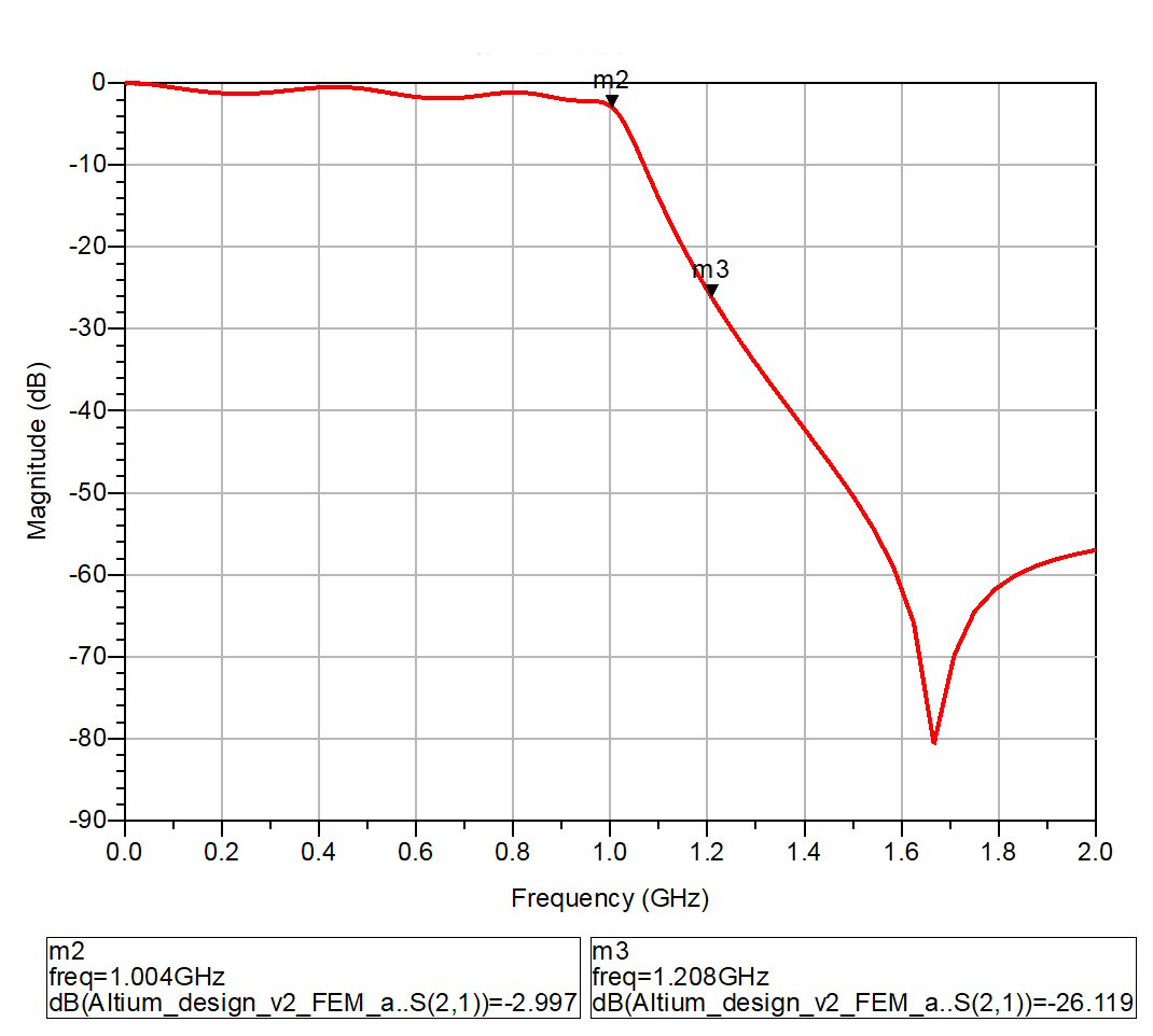
The first EM solver applied is MoM, via the Momentum simulator. The meshing frequency is set to 5 GHz with a meshing density of twenty cells/wavelength. The higher these two parameters are set, the finer the surface mesh, and typically the more accurate the results. Twenty cells/wavelength is the default meshing density value in Momentum. Momentum’s default meshing frequency is 2 GHz. This value is changed to 5 GHz to obtain more accurate results – at the cost of run time. Figure 9 shows |S21| and passband ripple.
9(a)

9(b)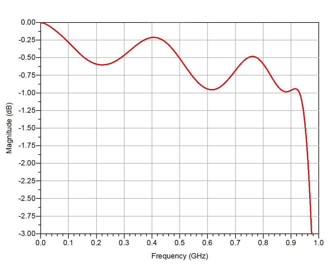
Fig. 9 Momentum (MoM) EM simulated results: |S21| with expanded scale in magnitude and frequency to show passband and rejection band (a) and |S21| with smaller scale to show passband ripple (b).
It is apparent that the results are different from the schematic simulations with a lower corner frequency and steeper roll-off. The corner frequency is at about 970 MHz with about 26 dB of attenuation at about 1.17 GHz (200 MHz past the corner). Another observation is how the stop band begins to roll back up at around 1.9 GHz. This is important because it shows how layout parasitics can potentially create a resonance around this frequency or change the filter dynamic. Also, observe that the passband ripple decreases to a relative minimum of about -1 dB before falling to the corner frequency. The total Momentum simulation duration is 2 minutes and 23 seconds.
FEM Simulated Results
The substrate lateral and vertical extensions are kept to the default values of 3.125 and 5 mm, respectively, while the substrate wall boundary is kept to the default open-type. These values create an open-air boundary around the layout design for finite element volumetric meshing. Within the meshing settings the delta error value is changed from the default 0.02 to 0.01 to further increase simulation accuracy; although, again, at the cost of run time. The consecutive passes of delta error is kept to 1 and the minimum/maximum number of adaptive passes are kept to 2 and 15, respectively. The consecutive passes of delta error refers to the number of consecutive times the delta error must be satisfied. Increasing this number ensures that the final solution is precise relative to the current finite element mesh refinement. The minimum/maximum number adaptive passes simply sets minimum/maximum numbers of runs, or attempts at satisfying the delta error, given the set boundary and meshing conditions. Figure 10 shows the FEM simulation results.
10(a)
10(b)
Fig. 10 FEM EM simulated results: |S21| with expanded scale in magnitude and frequency to show passband and rejection band (a) and |S21| with smaller scale to show passband ripple (b).
Again, it is apparent that the electromagnetic simulations differ from the schematic-based simulated results. The stop band is pushed forward in frequency with a slightly sharper roll-off. The corner frequency appears at nearly 1 GHz with about 3 more dB of attenuation (26 dB) observed at around 1.2 GHz. The passband ripple appears to fall off well below 0.5 dB before the corner frequency, generally varying between -0.5 and -2 dB.
Another observation is that the resonance and parasitic “roll-up” observed around 1.7 GHz is like the result observed in Momentum, but it is at 1.7 GHz as opposed to 1.9 GHz. The total FEM simulation duration is 2 minutes and 33 seconds and a delta error of 0.0014 is achieved.
Lab Measurements and Comparison
An Anritsu MS4622B Vector Network Analyzer (VNA) is used to measure the S-Parameters of the low-pass filter. A full 12-term calibration is performed from 10 MHz to 2 GHz prior to the measurement (10 MHz is the lowest measurable frequency on the VNA). Figure 11 shows the fabricated board design with measurement results shown in Figure 12.
11(a)
11(b)
Fig. 11 Fabricated filter circuit board assembly: front side (a), back side (b).
12(a)
12(b)
Fig. 12 Measured results: |S21| with expanded scale in magnitude and frequency to show passband and rejection band (a) and |S21| with smaller scale to show passband ripple (b).
The measured |S21| resembles the electromagnetic simulations with the resonance and parasitic “roll-up” observed around 1.7 GHz. The -3 dB corner frequency is at 944 MHz, with about 27 dB of attenuation measured 200 MHz past the corner, at 1.144 MHz. The passband ripple oscillates between -0.25 dB and -1.25 dB before falling to the corner frequency. The minimum stop-band attenuation is about -55 dB around 1.7 GHz before |S21| begins to increase.
Figures 13 and 14 show all four case results (schematic, MoM, FEM, and measurements) overlaid on the same plots. In both figures, the red trace represents the FEM simulator results, the blue trace represents the lab measured results, the magenta trace represents the Momentum (MoM) simulator results, and the green trace represents the schematic simulator results. All four cases share similarities, but also have specific differences.

Fig. 13 Comparative plot of |S21|.
 Fig. 14 Comparative plot of passband ripple.
In terms of accurately modeling the 3 dB corner frequency, the Momentum simulator is the closest at around 973 MHz compared to the measured 944 MHz. In terms of modeling the filter roll-off, both FEM and Momentum simulators are equally accurate. They both measure about 26 dB of attenuation, 200 MHz past their respective corner frequencies, while the lab measured data is around 27 dB of attenuation, 200 MHz past its corner frequency.
In terms of higher frequency stop-band modeling, the FEM simulator may have an advantage due to the location of the resonant and parasitic “roll-up.” Both the FEM simulator and measurements show this phenomenon around 1.7 GHz, while the Momentum simulator shows it at around 1.9 GHz. The schematic simulator does not show it at all.
Both the FEM and Momentum simulators adequately model ripple, although neither significantly outperforms the other, relative to the measured data. The FEM simulator predicts larger ripple, while the Momentum simulator predicts smaller ripple compared with the measured results.
Conclusion
Both FEM and MoM Electromagnetic solvers provide insight in the design of a low-pass filter. With only a 10 second difference in run time, both prove to be efficient and accurate. The FEM simulator more accurately models higher frequency parasitics that translate to resonances and a parasitic “roll-up” in insertion loss. Alternatively, the Momentum simulator more accurately models the filter’s -3 dB corner frequency.
The design under test, a microstrip-based filter, is composed of an inhomogeneous substrate (FR4) and two copper surface layers. The substrate properties may be more accurately modeled by the FEM solver due to its volumetric meshing techniques, while the surface traces and copper layers may be more accurately modeled by the MoM solver due to its surface current density meshing techniques.
Both FEM and MoM have their respective advantages and shortcomings. If working with a circuit that has several signal layers with vias or inhomogeneous materials, FEM may be more suitable. If working with a circuit that has only surface signal traces or planes, however, MoM may be a more efficient and an equally effective option. Nonetheless, both very accurately model practical, fabricated designs. It depends on the design, its application and its properties.
Acknowledgments
The author greatly appreciates Dr. Dean Arakaki and the Electrical Engineering Department of California Poly-technic State University, San Luis Obispo for their support and resources.
References
- D. B. Davidson, Computational Electromagnetics for RF and Microwave Engineering, Cambridge, 2011.
- C. A. Balanis, Advanced Engineering Electromagnetics, Wiley, 2012.
- “Advanced Design System 2017: Electromagnetic,” Keysight Technologies Software EDA Download. Web.