Wireless infrastructure designers must often contend with conflicting goals when developing new equipment for the base transceiver station (BTS) market. The components used in today's systems are frequently required to operate over multiple bands and under multiple modulation formats. The quest for higher performance, lower cost, component interchangeability and faster time to market seldom point to the same solution. This is especially true when selecting a low noise amplifier (LNA) for the receiver section of a BTS or cellular repeater.

The most popular device technology used in the front-end amplifier section of an infrastructure LNA is the GaAs-based pseudomorphic high electron mobility transistor (pHEMT). LNA assemblies based upon this device exhibit both low noise figure and high gain performance, which is well suited for applications within the wireless infrastructure frequency bands between 350 and 2200 MHz.

When selecting an LNA solution, the designer will generally use either a discrete assembly based on an unmatched transistor or a fully or partially matched plastic packaged MMIC LNA. The advantage of the discrete design is generally low noise figure, but the advantages of the more integrated MMIC approach include unit-to-unit consistency, ease of implementation, smaller PCB footprint and lower component count.
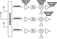
BTS receiver designs generally employ a low noise amplifier located as close as possible to the receive antenna, as depicted in Figure 1. After the antenna and receive filter, the next contributor to overall receiver noise figure is the first LNA stage. The noise figure contribution of stages subsequent to the LNA will be proportionally reduced by the gain of the LNA; therefore, it is important that the initial amplification stages of the receive chain offer high gain and low noise figure. This strategy will result in the highest possible dynamic range of the receiver.

BTS receivers must be able to reliably receive signal levels from subscriber units, which can range from less than -120 dBm to as high as -20 dBm. The designer strives to insure that the receiver can meet the desired performance with as low an input signal as possible, while being careful not to overdrive the first mixer stage. The first downconverter mixer typically has an input third-order intercept point (IP3) in the range of +30 to 38 dBm and the architecture is chosen so that the maximum signal levels to the mixer will be well below its compression point in order to minimize spurious issues.
Hittite Microwave has introduced four high IP3 pHEMT MMIC LNAs for wireless infrastructure receiver applications. Table 1 summarizes the performance of the LNA product line covering all cellular and 3G applications from 350 to 2200 MHz. The HMC356LP3, HMC372LP3 and HMC375LP3 devices are standard LNAs, while the HMC373LP3 offers an LNA with an integrated low loss bypass mode. Each of these unconditionally stable LNAs provide very consistent performance over temperature and are self biased from a single positive 5 V supply. A minimum of external components is required, including a single shunt inductor to optimize the input match while the output is matched to 50  and is internally DC blocked.

All four LNAs are assembled into low cost 3 x 3 x 1 mm surface-mount (SMT) leadless QFN plastic packages, designated as LP3. The QFN package is fully compatible with automated assembly and reflow soldering processes. The products are manufactured on a qualified, production GaAs pHEMT wafer process. These new high dynamic range LNAs complement the company's high IP3 mixer, gain block and control device product offerings giving the BTS and repeater designer a complete set of receiver IC component solutions to choose from.
|
Table 1 | |||||
|
|
HMC356LP3 |
HMC372LP3 |
HMC373LP3 |
HMC375LP3 | |
|
LNA Mode |
Bypass Mode | ||||
|
Frequency (MHz) |
350 to 550 |
700 to 1000 |
700 to 1000 |
700 to 1000 |
1700 to 2200 |
|
Noise figure (dB) |
1.0 |
<1.0 |
0.9 |
2.0 |
0.9 |
|
Gain (dB) |
17.5 |
14.5 |
14.0 |
-2.0 |
17.0 |
|
Input return loss (dB) |
18 |
25 |
25 |
30 |
13 |
|
Output return loss (dB) |
16 |
13 |
12 |
25 |
15 |
|
Output P1dB (dBm) |
+21 |
+21 |
+21 |
+30 |
+18.5 |
|
Output IP3 (dBm) |
+38 |
+34 |
+35.5 |
+50 |
+33.5 |
|
Supply current |
104 |
100 |
90 |
0.010 |
136 |

HMC356LP3 350 to 550 MHz LNA
The HMC356LP3 high IP3 LNA was designed for GSM 450/480 and CDMA 450 cellular base station and mobile radio front-end receiver applications between 350 and 550 MHz. Figure 2 plots the amplifier's typical performance of 1.0 dB noise figure and 17.5 dB gain. As seen in Figure 3, the +38 dBm typical output IP3 only varies ±1.5 dB over the standard commercial ambient temperature range of -40 to +85°C. Input and output return losses are outstanding at 18 and 16 dB, respectively, with the LNA requiring only four external components. The HMC356LP3 shares the same package and RF/DC pin out with the HMC372LP3 high IP3 LNA.
HMC372LP3 700 to 1000 MHz LNA

The HMC372LP3 high IP3 LNA was designed for GSM and CDMA cellular base station front-end receivers operating between 700 and 1000 MHz. This amplifier offers typical performance of less than 1.0 dB noise figure, 14.5 dB gain and +34 dBm output IP3 from a single supply voltage. Figure 4 demonstrates how the gain, P1dB and noise figure performance of the HMC372LP3 is constant over a ±10 percent supply voltage tolerance. Since the product family shares similar MMIC circuitry, this consistent performance is indicative of the behavior of the other MMIC LNAs. The output IP3 is fairly constant and better than +34 dBm for input power up to -3 dBm per tone yielding outstanding dynamic range, as shown in Figure 5. Input and output return losses are excellent at 25 and 13 dB, respectively, with the LNA requiring only four external components.

HMC375LP3 1.7 to 2.2 GHz LNA
The HMC375-LP3 high IP3 LNA was designed for applications in GSM, EDGE, CDMA and W-CDMA base station front-end receivers operating between 1.7 and 2.2 GHz. Figure 6 shows that this amplifier offers an excellent typical mid-band noise figure of 0.9 dB combined with 17 dB gain. Figure 7 shows that the typical +33.5 dBm output IP3 is very consistent at ±0.5 dB over the standard +5 V supply voltage tolerance of ±10 percent across the PCS/3G frequency band. The other MMIC LNAs in the product family share this same consistent IP3 performance trait. The HMC375LP3 uses the same RF input and output pins as the HMC356LP3 and HMC372LP3 to help BTS designers "standardize" their RF receiver PCB card layouts from system to system.

Implementation of the Standard MMIC LNAs
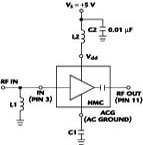
Figure 8 depicts the simple application circuit of the HMC356LP3, HMC372LP3 and HMC375LP3 standard LNAs. The only two required external RF matching components are a shunt chip inductor on the RF input line to optimize the RF input match and a shunt capacitor which provides an RF ground to the source of the active device on the AC ground (ACG) pin.
The Vdd supply voltage is fed to the device through a series L and shunt C configuration in order to isolate the DC supply from the RF path within the amplifier. These components are standard off-the-shelf inductor and capacitor values and tolerances. Each data sheet for these products gives a recommended set of L and C values for the respective operating bands.
When compared to a discrete pHEMT-based assembly, for example, the HMC372LP3 700 to 1000 MHz LNA requires only four external components and 38 mm2 of PCB area, while a comparable discrete transistor-based solution requires 17 components, and approximately 180 mm2 of PCB area. This represents a savings of approximately 75 percent of the PC board area required for the LNA when using the HMC372LP3 MMIC LNA.

LNA assemblies based upon discrete depletion mode devices require both a positive and a negative voltage supply, further complicating the PCB layout and the stabilization of the small and large signal performance over temperature.
The MMIC LNA approach simplifies the tasks of temperature stabilization and of balancing the performance between multiple channels on a BTS receiver by virtue of the inherent unit-to-unit consistency of an IC design. MMIC-based LNAs offer excellent repeatability, higher reliability, simplified power and gain control, while minimizing the material list for the BTS receiver. Figure 9 shows the compact size of the HMC372LP3 with its required matching components on a standard evaluation PCB.
HMC373LP3 700 to 1000 MHz LNA with Integrated Bypass Mode

The HMC373LP3 is a versatile, high dynamic range GaAs MMIC LNA that integrates a low loss bypass mode on the IC. The amplifier is ideal for GSM and CDMA cellular base station front-end receivers operating between 700 and 1000 MHz where the BTS or repeater designer is concerned that a received subscriber signal level may become large enough to cause the LNA to overdrive the down converting mixer. The bypass mode can be activated in that case allowing the signal to be diverted though a low loss path and into the mixer.
The HMC373LP3 LNA combines an excellent 0.9 dB noise figure with 14 dB of gain and +35.5 dBm output IP3 from a single supply of +5.0 V at only 90 mA. Figure 10 shows the very stable noise figure performance of ±0.1 dB over the commercial operating temperature range of -40° to +85°C. Input and output return losses are 28 and 12 dB, respectively.

Figure 11 depicts the HMC373LP3 application circuit. The HMC373LP3 LNA operates normally when pin 4 (Vctl) is presented with a low resistance path to ground. The bypass feature of the LNA is activated and the LNA shut down by removing the DC path from Vctl to ground. An external 1000 pF shunt capacitor connected to Vctl provides an RF ground to the device for both modes. In bypass mode, the HMC373LP3 exhibits 2 dB of insertion loss with better than 20 dB return loss, as shown in Figure 12, while consuming less than 10 µA of supply current. The HMC373LP3 can be dynamically switched between LNA mode and bypass mode by connecting a MOSFET switching device to Vctl. Devices such as the Zetex ZXM61N02F are widely available at very low cost.
Conclusion
A family of high dynamic range MMIC LNA products has been introduced that enable cellular/3G BTS and repeater designers to simplify their front-end receiver amplification circuits. The LNAs are easy to use, combine excellent noise figures of 0.9 to 1 dB with high output IP3 of +33 to +38 dBm and offer consistent, reliable MMIC construction.

The high IP3 feature of these amplifiers make them particularly well suited in applications where the output of the LNA is fed directly into a high IP3 mixer, or in applications where the LNA is succeeded by a high loss device such as a multi-way splitter, or high range digital attenuator.
Data sheets and de-embedded S-parameter files for each device are available at www.hittite.com. Product samples and tested evaluation PCBs may be ordered on-line. Sample and production quantities are available from stock.
Hittite Microwave Corp., Chelmsford, MA (978) 250-3343. Circle No. 303
