Indian researchers have developed a high performance industry-standard model for aluminum gallium nitride (AlGaN/GaN) high electron mobility transistors (HEMTs) with simple design procedures which can be used to make high-power RF circuits owing to its high breakdown voltage.
RF circuits include amplifiers and switches, which are used in wireless transmission and are useful for space and defense applications.
As AlGaN/GaN HEMTs can also extend the power level of solid-state microwave circuits by a factor of five to ten, resulting in an appreciable reduction in the overall chip size and cost, the standard developed can significantly reduce the development cost of the circuits and devices for transmitting high frequency signals.
The technology is rapidly gaining popularity owing to its high performance and efficiency. It has two excellent properties—high mobility and high-power performance. These properties reduce the noise figure and complexity while designing low noise amplifiers (LNAs) while increasing the achievable bandwidth.
AlGaN/GaN HEMTs have become the technology of choice for high frequency and high-power applications like 5G, radars, base stations, satellite communications, etc. To design wideband power amplifiers, a fully robust and accurate physics-based RF GaN HEMT model is of prime importance.
In the current work, the team led by Prof. Yogesh Singh Chauhan at IIT Kanpur developed and standardized a physics-based compact model for AlGaN/GaN HEMTs—the Advanced Spice Model for GaN HEMTs (ASM-HEMT). The standard model for circuit design developed simplifies the design procedure for high performance RF circuits and helps in automating the design efforts as well as brings down the overall development cost. Besides, it can accurately predict the AlGaN/GaN HEMT's behavior in circuit design.
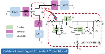
 A small-signal equivalent of the industry-standard ASM-HEMT model.
The development of the model involved characterizing AlGaN/GaN HEMTs using state-of-the-art characterization systems integrated in a setup used for measuring the electronic characteristics like current, the capacitance of semiconductor devices, including high frequency characteristics. This setup (consisting of a Keysight B1500 Semiconductor Device Analyzer, an AMCAD PIV system, a passive load-pull system from Maury Microwaves, a Keysight B1505 Power Device analyzer, all connected using a FormFactor probe station) was partially supported by ‘Fund for Improvement of S&T Infrastructure’ (FIST) and Technology Development Programme (TDP) schemes of the Department of Science and Technology.
The measurements facility funded by FIST & TDP is being heavily used by ISRO, DRDO and other companies to characterize the semiconductor devices for high frequency applications.
Prof. Chauhan’s team measures the current, capacitance and RF characteristics of the devices under test and uses parameter extraction tools to extract the parameters of the ASM-HEMT model for a given technology. Once the model behavior is in close agreement with the measured characteristics, the model is validated for practical applications.
 Large-signal load-pull contours modeled accurately using the industry-standard ASM-HEMT model.
The team is concurrently working on circuit design and has delivered a state-of-the-art commercial GaAs-based LNA with one of the lowest reported noise figures in the market. Ongoing efforts include LNA and PA design based on the AlGaN/GaN material system.

