
Small-signal measurements are conducted using a Keysight E5247 network analyzer (see Figure 5a). The input port of the circuit is designed to match with 50 Ω at 24 GHz. The 3 dB bandwidth is about 6 GHz from 21.1 to 27.1 GHz, while 14.6 dB peak gain is achieved at 23.5 GHz. S11 is lower than -10 dB from 22 to 25.4 GHz with S22 around -5 dB without an output matching network. S12 of the PA across the 20 to 30 GHz band is lower than -38 dB, which indicates a high level of reverse isolation.
Large-signal measurements (see Figure 5b) show output power, power gain and PAE. The PA can produce 14.2 dBm of saturated output power with 10.5 dBm OP1dB at 23.5 GHz. The measured maximum output power is slightly lower than simulated due to parasitic effects. The maximum PAE is 23.5 percent.
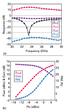
Figure 5 PA small- (a) and large-signal (b) performance.
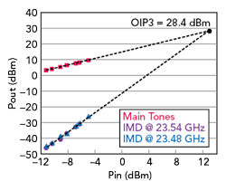
Figure 6 PA two-tone measurements and calculated OIP3.
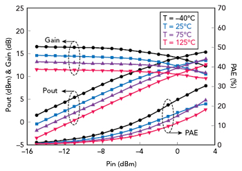
Figure 7 Measured output power, gain and PAE over temperature.
Two-tone measurements verify the linearity. The two tones are applied at 23.5 GHz and 23.52 GHz using analog signal generators. The signals are combined through a magic tee and the outputs are captured by a signal analyzer. Figure 6 shows the linearity of the PA and measured OIP3 of 28.4 dBm. This is 14.4 dB higher than reported by Komijani et al.,6 for a PA in bulk CMOS. This demonstrates that PAs with high linearity can be achieved using trap-rich SOI-CMOS technology.
A high and low temperature semiautomatic probe station is used to measure RF performance at different temperatures (see Figure 7). Output power, gain and maximum PAE for the PA at -40°C are 15.4 dBm, 16.7 dB and 30.2 percent, respectively. A slightly degeneration in RF performance is observed at 125°C, but the chip can still provide a peak gain of 11.5 dB, an output power of 12.6 dBm and a peak PAE of 18.3 percent.
PA gain for devices fabricated in bulk CMOS reported by Dawn et al.5 shows 7.7 dB degeneration at 80°C compared with room temperature. This PA designed in trap-rich SOI-CMOS technology demonstrates superior temperature performance without any temperature compensating circuits. It is an important consideration for automotive electronics applications where cooling is inappropriate or not possible.
CONCLUSION
A K-Band stacked-FET PA in 90 nm trap-rich high-resistance SOI-CMOS technology with high linearity and superior temperature stability uses a two-stacked-FET architecture and low loss coplanar waveguide matching networks to improve the RF output power and PAE. Dummy fills in the lower layer are removed to minimize the influence on CPW lines and multi-turn inductors. Sizes of stacked MOSFETs are optimized to omit the output matching network and reduce chip area.
ACKNOWLEDGMENT
This work was supported by the National Key Research and Development Program of China under Grant No. 2016YFA0202304 and 2016YFA0201903, General Program of National Natural Science Foundation of China under Grant No. 61674168 and 61504165, as well as the Opening Project of Key Laboratory of Microelectronics Devices and Integrated Technology, Institute of Microelectronics, Chinese Academy of Sciences.
References
- Y. Kim, S. Lee and Y. Kwon, “45 GHz Stacked-FET PA with Linearizing Feed-Forward Rectifier,” Electronics Letters, Vol. 52, No. 18, July 2016, pp. 1535–1537.
- D. P. Nguyen, T. Pham, B. L. Pham and A. V. Pham, “A High Efficiency High Power Density Harmonic-Tuned Ka Band Stacked-FET GaAs Power Amplifier,” IEEE Compound Semiconductor Integrated Circuit Symposium, October 2016.
- I. Gresham, A. Jenkins, R. Egri, C. Eswarappa, F. Kolak, R. Wohlert, J. Bennett and J. P. Lanteri, “Ultra Wide Band 24 GHz Automotive Radar Front-End,” IEEE MTT-S International Microwave Symposium Digest, June 2003, pp. 369–372.
- H. T. Dabag, B. Hanafi, F. Golcuk, A. Agah, J. F. Buckwalter and P. M. Asbeck “Analysis and Design of Stacked-FET Millimeter-Wave Power Amplifiers,” IEEE Transactions on Microwave Theory and Techniques, Vol. 61, No. 4, April 2013, pp. 1543–1556.
- D. Dawn, S. Sarkar, P. Sen, B. Perumana, M. Leung, N. Mallavarp, S. Pinel and J. Laskar, “60 GHz CMOS Power Amplifier with 20-dB Gain and 12 dBm Psat,” IEEE MTT-S International Microwave Symposium Digest, June 2009, pp. 537–540.
- A. Komijani, A. Natarajan and A. Hajimiri, “A 24-GHz, +14.5 dBm Fully Integrated Power Amplifier in 0.18-μm CMOS,” IEEE Journal of Solid-State Circuits, Vol. 40, No. 9, October 2005, pp. 1901–1908.
- S. Shakib, H. C. Park, J. Dunworth, V. Aparin and K. Entesari, “A 28 GHz Efficient Linear Power Amplifier for 5G Phased Arrays in 28nm Bulk CMOS,” IEEE International Solid-State Circuits Conference, January-February 2016, pp. 352–353.
- A. Tsuchiya and H. Onodera, “Effect of Dummy Fills on Characteristics of Passive Devices in CMOS Millimeter-Wave Circuits,” IEEE 8th International Conference on ASIC, October 2009, pp. 296–299.