Due to the fast growing demand for broadband wireless communications, the operating frequency is moving toward the 5 GHz U-NII band. With a maximum data rate of 54 Mbps, the IEEE 802.11a wireless LAN (WLAN) standard specifies a 300 MHz allocation of spectrum in the 5 GHz range that is divided into three sub-bands, as shown in Figure 1 .1

The lower and middle U-NII sub-bands, from 5.15 to 5.35 GHz, accommodate eight channels in a total bandwidth of 200 MHz. The 100 MHz bandwidth of the upper U-NII band, from 5.725 to 5.825 GHz, accommodates four channels. The 100 MHz lower U-NII band is restricted to a maximum power output of 40 mW, and the middle and upper sub-bands are restricted to 200 and 800 mW, respectively. The 802.11a WLAN frequency allocation overlaps with HIPERLAN from 5.15 to 5.3 GHz.
The proposed heterodyne transceiver architecture for an 802.11a WLAN application (5.725 to 5.825 GHz) is shown in Figure 2 . In the receive mode, the RF (5.725 to 5.825 GHz) is downconverted to a 200 MHz IF with a high side LO (5925 to 6025 MHz).

In addition, the center frequency is translated to zero by a 200 MHz LO to produce the I and Q baseband components. In the transmit mode, the I and Q baseband signals are first upconverted to 280 MHz and combined together, and then upconverted to RF by a 6.005 to 6.105 GHz LO.
The advantage of combining baseband and the RF front-end on one single chip for cost savings is strongly desired for highly integrated systems-on-chip (SOC) applications. Recently, many RF circuits realized in the CMOS process have been reported and the 0.18 µm process is a good candidate for highly integrated SOC applications.
The requirements of low power and low cost push the trend toward a single radio chip. A fully-integrated voltage-controlled oscillator (VCO) is one of the most important and challenging building blocks in an RF transceiver. With the demand for low power and low cost, an on-chip VCO with no external components is the best choice. However, the low Q on-chip passive components such as inductors will degrade the VCO phase noise performance.

This article presents a fully-integrated 5 GHz VCO fabricated by a TSMC 0.18 mm standard CMOS process. The VCO output frequency covers the 5925 to 6025 MHz range and is applicable to the front-end receiver with an IF of 200 MHz with a high side LO.
Circuit Design
The transistor's flicker noise (1/f) is the cause of the phase noise near the carrier with a 1/f3 shape. In the CMOS process, the transistor's 1/f noise is generally high, causing serious degradation of VCO phase noise performance. However, the PMOS 1/f noise is usually lower than for the NMOS by one order of magnitude.
A low 1/f noise active port reduces not only the magnitude of phase noise in the 1/f3 and 1/f2 regions, but also lowers the corner frequency between the 1/f3 and 1/f2 regions. To obtain better phase noise performance, PMOS transistors were used in the VCO core.2
The circuit and layout of the VCO, fabricated by the 0.18 µm CMOS process with a chip area of 790 x 1020 µm2 including pads, is shown in Figure 3 . The Agilent Advanced Design System (ADS) is used for design simulation of the VCO. The cross-coupled connection of the PMOS transistors M1 and M2 form a positive feedback loop to provide negative resistance to compensate for the loss in the L-C tank circuit.

The source and gate voltages of M1 and M2 are 0 V and VDD (1.8 V), respectively, without any extra current source. This bias scheme reduces the transistor width requirement for the oscillation to start and maximizes the oscillator signal peak-to-peak amplitude. The supply voltage for the 0.18 µm standard CMOS process is 1.8 V, which is fairly small.
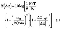
If the cross-coupled pair is biased via a current source, the allowable oscillator voltage swing will be further restricted and cause a poorer phase noise performance. According to the Leeson-Cutler phase noise model, the phase noise, which is the ratio of single-sideband-noise to carrier, is inversely proportional to the signal power.2


For low supply voltage operation, enlarging the voltage swing by removing the use of a current source, which reduces the voltage headroom, is one of the most direct ways to improve the phase noise performance, since the tank Q is primarily limited by the process.
As shown in Figure 4 , the tail current source not only limits the VCO voltage swing but also degrades the phase noise performance as well. If the VCO differential pair is unbalanced, the common-mode node of the current source will oscillate at twice the oscillation frequency.
Through channel length modulation, the noise from the current source will be upconverted to twice the oscillation frequency. The upconverted noise at twice the oscillation frequency enters the VCO core circuit and mixes with the fundamental frequency, and results in phase noise at the oscillation frequency.

To further suppress the phase noise in the 1/f3 region, caused by the MOS 1/f noise, the oscillation waveform must be made as odd-symmetric as possible.3,4 The 1/f noise of the active device will be upconverted to become 1/f3 noise when the VCO waveform is not sufficiently odd-symmetric. Therefore, the waveform symmetry must be taken care of when designing a VCO, especially with such a high 1/f noise device as MOS.
The L-C resonator is formed by on-chip spiral inductors (L1 and L2), p+/n-well junction varactors (Cv) and capacitors (C1 and C2). The Q-factor of the tank circuit is primarily limited by the inductor Q, which is approximately 10 at 5 to 6 GHz.
The inductors are 2.5 turn, rectangular spirals using thick AlCu metal (Metal-6) and their inductance is approximately 2.3 nH. The series connections, C1-Cv and C2-Cv, resonate with L1 and L2, respectively, to determine oscillation frequency.

The VCO output frequency is tuned by applying a control voltage of 0 to 1.8 V at the n-well terminal of the reverse biased junction varactors. M3 and M4 form open drain buffer amplifiers in order to drive 50 Ω test systems, such as a spectrum analyzer.
Measured Results
The VCO measurements are performed on an FR-4 PCB test fixture. The VCO chip is connected to the test board with aluminum bond-wires. The effects of the bond-wires and the FR-4 test board are all taken into account in the simulations.
The bond-wires and the FR-4 test board do not affect the oscillation frequency and phase noise performance; they only lower the output signal amplitude. The VCO core and each buffer amplifier dissipate 8.1 mW and 22.5 mW from a 1.8 V supply, respectively.

The measured oscillation frequency of the VCO is 5860 to 6026 MHz when the control voltage varies from 0 to 1.8 V. The VCO tuning range measurement and simulation results are shown in Figure 5 . The measured output power is approximately -4 dBm, as shown in Figure 6 .
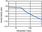
The phase noise at a 300 kHz offset from the carrier is measured to be -95.6 dBc/Hz, as shown in Figure 7 . The VCO phase noise measurement is performed when the applied control voltage is 0 V, which is when the VCO has its highest tuning sensitivity Kvo (approximately 180 MHz/V) and therefore where the measured phase noise is the worst.
The free running measured phase noise performance proves that the fully-integrated VCO is adequate for wireless communications. When the VCO is used in future 5 GHz frequency synthesizer applications, the phase noise can be further suppressed by the loop filter of the PLL frequency synthesizer. The output spectrum of the VCO is shown in Figure 8 .

The second harmonic is lower than the fundamental by 41.6 dBc, which implies that the VCO pull up and pull down waveform is highly odd-symmetric. The photograph of the FR-4 PCB test fixture is shown in Figure 9 . Table 1 summarizes the measured performance of the designed 5 GHz CMOS VCO.
Conclusion
A fully-integrated 5 GHz L-C tank VCO, fabricated in a TSMC 0.18 µm standard CMOS process, is presented. Made for an IEEE 802.11a WLAN application (5.725 to 5.825 GHz), the VCO output frequency covers 5925 to 6025 MHz and is adequate for the front-end receiver application, with an IF of 200 MHz and a high side LO.
The VCO core circuit uses only PMOS to achieve better phase noise performance. The VCO output frequency is tuned by on-chip p+/n-well junction varactors. The measurements are performed using an FR-4 PCB test fixture. The output frequency of the VCO is from 5860 to 6026 MHz with a 166 MHz tuning range, and the phase noise is -95.6 dBc/Hz at a 300 kHz offset.
The VCO, excluding buffer amplifiers, consumes 8.1 mW at VDD = 1.8 V. The low power consumption of the VCO suggests that the 0.18 µm CMOS process is useful for 5 GHz WLAN applications.
Acknowledgement
The authors would like to thank the Chip Implementation Center (CIC) of the National Science Council, Taiwan, ROC, for supporting the TSMC CMOS process.
Reference
1. IEEE Standard 802.11a: High Speed Physical Layer in the 5 GHz Band, 1999.
2. C.M. Hung, B.A. Floyd, N. Park and K.K. O, "Fully-integrated 5.35 GHz CMOS VCOs and Prescalers," IEEE Transactions on Microwave Theory and Techniques , Vol. 49, No. 1, January 2000, pp. 17-22.
3. A. Hajimiri and T.H. Lee, "Oscillator Phase Noise: A Tutorial," IEEE Journal of Solid-State Circuits , Vol. 32, No. 3, March 2000, pp. 326-336.
4. T.H. Lee, The Design of CMOS Radio-frequency Integrated Circuits , Cambridge University Press, New York, NY 1998.
