
Figure 8 shows a 3D view, the entire layout and the fabricated PA circuit. Both varactors are placed on the input side of the PA. Two additional DC blocking capacitors separate the transistor bias from the varactor bias. Figure 9 shows the simulated S11 of the output matching network, highlighting the two band of interest: 1.5 and 5 GHz. Load-pull analysis15 determined the optimal power and efficiency of the 1.25 mm GaN device, and the ΓL data was used as the initial starting point for the design of the concurrent dual-band PA.
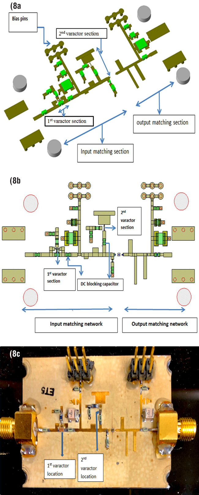
Figure 8 3D (a) and layout (b) views and fabricated (c) PA circuit, showing the locations of the two varactor sections.
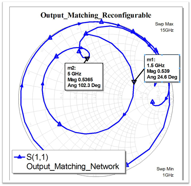
Figure 9 Output matching network S11.
The on and off simulations of |S11| and |S21| for the first and second varactor sections are presented in Figures 10 and 11, respectively. For the first varactor section (see Figure 10), with 0 V bias, the minimum |S21| is –36.4 dB at 4.4 GHz, representing a capacitance of 4 pF. With 8 V bias, the minimum |S21| is –18.4 dB at 8.0 GHz, representing a capacitance of 0.8 pF. For the second varactor section, with 0 V bias, the minimum |S21| is –14.7 dB at 1.7 GHz, representing a capacitance of 4 pF. Biased on, the minimum |S21| is -16.6 dB at 3.5 GHz, representing a capacitance of 0.8 pF. The varactors create notches at different frequencies, determined by the bias voltage. This characteristic, along with placement of the varactors in the input matching section of the circuit, enables the desired band rejection.
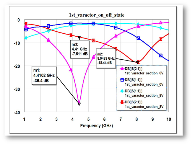
Figure 10 On/off characteristics of the first varactor section.
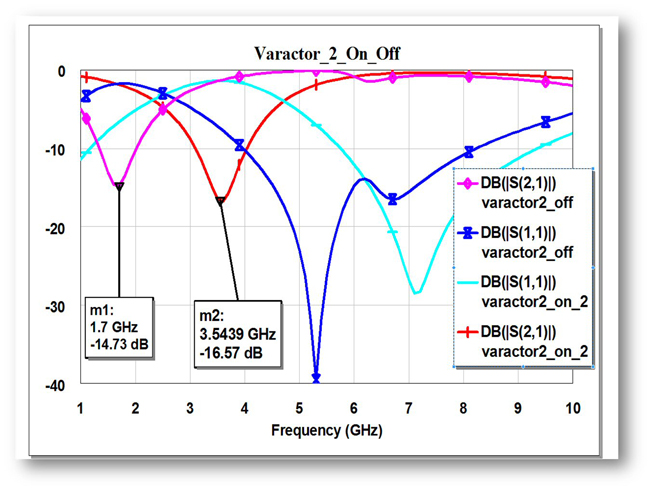
Figure 11 On/off characteristics of the second varactor section.
The entire input network and its simulated S22 are shown in Figure 12.
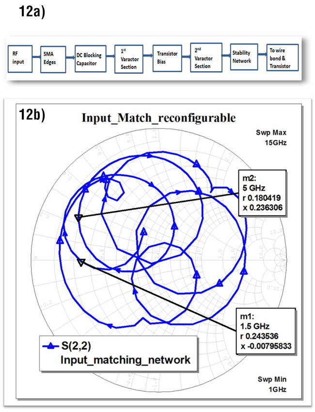
Figure 12 Input network (a) and simulated S22 (b).
DUAL-BAND PA PERFORMANCE
Figure 13 shows the simulated small-signal performance of the dual-band design. To achieve dual-band performance, both varactors are biased so their capacitance values are 0.8 pF. At this bias, the small-signal gain is 14.1 dB at 1.4 GHz and 15.4 dB at 5 GHz, with the input return loss better than 7 dB at L-Band and 6 dB at C-Band. The output return loss is better than 13 dB for both bands.
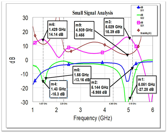
Figure 13 Small-signal simulation of the dual-band PA.
Figure 14 shows the simulated large-signal performance in dual-band operation, i.e., with both varactors biased to 0.8 pF. At L-Band, the simulation predicts a PAE of 51.9 percent, Pout of 33.8 dBm and a compressed gain of 10.8 dB. At C-Band, the simulation predicts a simultaneously PAE of 62.8 percent, Pout of 36.2 dBm and compressed gain of 13.4 dB. The PA achieves good performance in both bands.
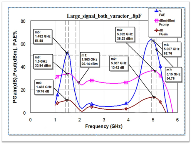
Figure 14 Large-signal simulation of the dual-band PA.
Figures 15 and 16 show the simulated large-signal performance with only one of the two bands selected, i.e., the other rejected.
L-Band operation is shown in Figure 15, with a simulated peak PAE of 53.1 percent, an output power of 34.2 dBm and associated gain of 11.1 dB. The gain at C-Band is less than 3 dB, with PAE less than 10 percent and output power less than 22 dBm.
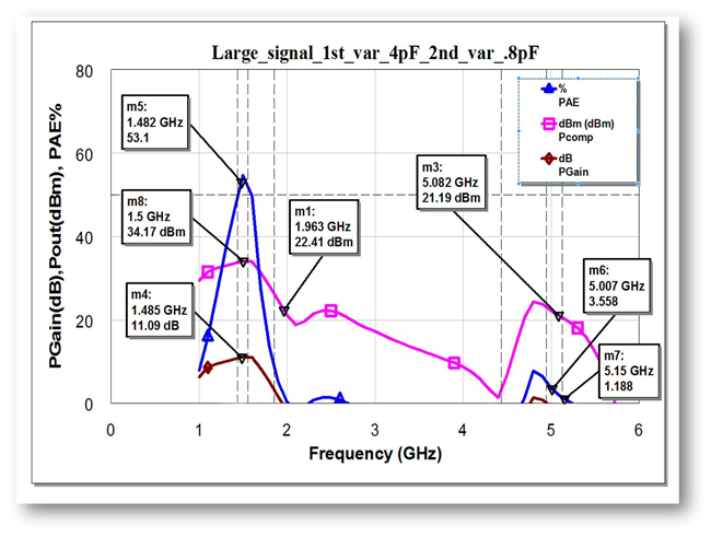
Figure 15 Large-signal simulation with L-Band selected: PAE, Pout and saturated gain vs. frequency.