
A reconfigurable, dual-band, high efficiency power amplifier (PA) employing 0.25 μm GaN technology simultaneously covers two distinct telemetry bands: L (1.435 to 1.55 GHz) and C (5.0 to 5.15 GHz). The uniqueness of this design is its three modes. Either one of the bands can be eliminated simply by applying a bias voltage to a barium strontium titanite (BST) varactor. High efficiency, high output power and high gain are achieved.
RF PAs are used in a wide variety of applications including cell phones, wireless communications, radar and electronic warfare (EW). Reconfigurability, where the same hardware can be used for different frequency bands, is important to meet the needs of future wireless systems. To efficiently manage spectrum use and meet future Department of Defense (DoD) requirements, agile reallocation of wireless assets to less congested bands is becoming essential.
In the United States, specific frequency bands are allocated for telemetry.1 For this development effort, the L and C bands are the ones of interest. The DoD is auctioning off the L (1.435 to 1.85 GHz) and S (2.2 to 2.395 GHz) bands for commercial applications and moving to C-Band (4.4 to 6.7 GHz). Most existing systems, however, still use the legacy L and/or S bands. To ensure compatibility with both the legacy and new systems, it is preferred to use a dual-band design, as the telemetry transmitters must be interchangeable between bands and require no modifications to the aircraft. The PAs are key components, so proper PA design to accommodate multi-band operation is a requirement.
The challenge of multi-band and multi-standard operation can be met with reconfigurable technologies. Various approaches using CMOS switches,2 MEMS switches,3 PIN diodes,4 thin film BST capacitors,5 high Q varactor diodes,6 GaN RF switches7 and integrated piezoelectric actuators8 have been used for reconfigurable PA designs. In most of these earlier research efforts, the reconfigurable PAs were designed for applications other than telemetry. The design described here addresses the demand and importance of reconfigurable PAs in the L and C telemetry bands used for EW applications.9 The unique feature of the design is its simplicity, where tunable components are used only in the input matching network to select one of the bands of the concurrent dual-band PA.
The increasing need for high power at RF/microwave frequencies led to the development of compound (III-V) semiconductor GaAs and GaN transistors, which are useful for microwave PAs because of their high electron mobilities.10,11 Because of their exceptionally high power density and breakdown voltage, GaN high electron mobility transistors (HEMT) are being rapidly adopted for various applications.12 The high thermal conductivity of SiC efficiently dissipates the excess heat of the high power density devices, preventing extreme channel temperature and reduced reliability. For this work, a Qorvo 5 W GaN on SiC HEMT was used.
The reconfigurable behavior of the PA was accomplished by exploiting the unique structure of a BST varactor, in which a thin BST layer is sandwiched between two metal plates. Ferroelectric materials like BST are dielectrics with complex functionalities. Some of their physical properties, such as permittivity and polarization, change with variations in the external electromagnetic field, temperature and mechanical strain, and these functionalities can be used for various applications. In this design, a unique coplanar waveguide BST varactor13 was used to achieve dual- and single-band operation.
DESIGN OVERVIEW
The design approach was a concurrent dual-band PA operating in the L and C telemetry bands, with a notch to reject one of the bands (see Figure 1). Two BST varactors are used to create rejection notches at the specified frequencies, with the selected frequency depending on the capacitance values of the varactors. The capacitance values are controlled by the applied bias voltages, which are switchable to select one of the two bands (i.e., L or C).
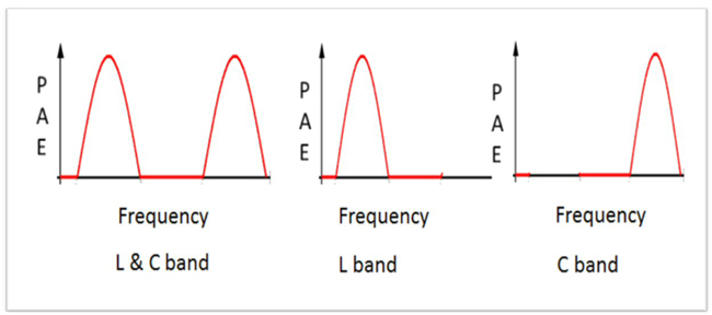
Figure 1 Three PA operating states: dual-band or either L or C.
Figure 2 shows the electrical model of the BST thin film varactor. Biased with a fixed voltage, the varactor is modeled using lumped elements as a conventional parallel-plate capacitor, where the capacitor C1 represents the BST capacitor, and the parallel resistor R1 represents the dielectric loss of the ferroelectric material. The series resistance R represents the parasitic conductor and interconnect (i.e., electrode) resistance, and the series inductor L1 represents the parasitic presented by the shunt line in the varactor.
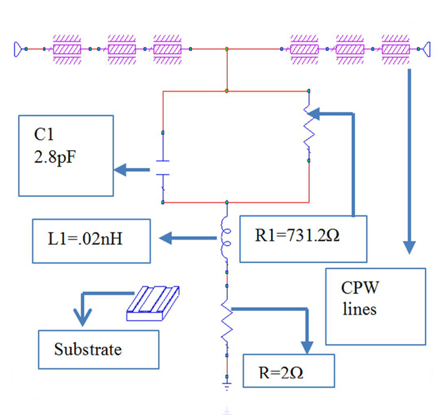
Figure 2 BST varactor model.
With no bias voltage applied, the varactor is “off,” its effective capacitance is highest, and the signal is shunted to ground instead of appearing at the output port. As DC bias is applied, the varactor turns “on,” and its capacitance decreases, which allows more signal to pass from the input to the output. This feature is used to create a notch filter to reject one of the bands.
Simulation of the BST varactor with bias is shown in Figure 3, with |S21| and |S11| values of -0.88 and -10 dB, respectively, at 3 GHz. The simulated |S21| and |S11| without bias is shown in Figure 4. In this case, the |S21| and |S11| values are -7.2 and -1.71 dB, respectively, at 3 GHz.
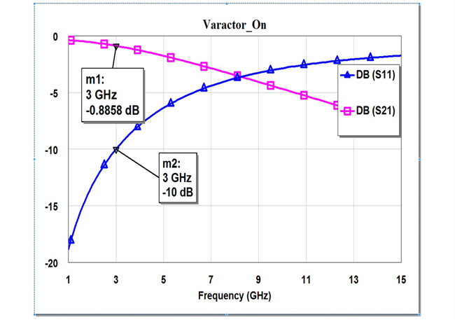
Figure 3 Simulated |S21| and |S11| vs. frequency for a single varactor when biased on.
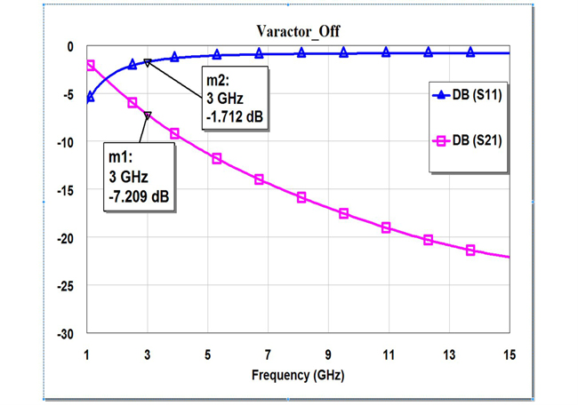
Figure 4 Simulated |S21| and |S11| vs. frequency for a single varactor when off.
PA DESIGN
The PA circuit uses one transistor assembled on a Rogers TMM4 substrate, which has a thickness of 15 mils, a dielectric constant of 4.5 and a copper metal thickness of 0.7 mils.9 The 5 W Qorvo GaN transistor selected for the design has a breakdown voltage of 100 V, maximum drain voltage rating of 40 V and maximum drain current of 1.25 A.14
The dual-band PA was designed using Cadence® AWR® Microwave Office® and implemented in a hybrid configuration. A Modelithics transistor model was used for the Qorvo 5 W device, and load-pull analysis determined the optimal power and efficiency of the transistor.15,16 Figure 5 shows the load-pull contours at 1.5 GHz, with power-added efficiency (PAE) shown in blue, output power (Pout) in pink; the contours at 5 GHz are shown in Figure 6. For these tests, the device was biased at VDS = 28 V and VGS = -2.7 V. For optimal efficiency at 1.5 GHz, Figure 5 show a load reflection coefficient ΓL = 0.3 at an angle of 40.8 degrees, resulting in a PAE of 66.9 percent and an associated Pout of 38 dBm. The load-pull analysis at 5 GHz yields ΓL = 0.5 at an angle of 89.1 degrees, resulting in a PAE of 66.2 percent with an associated Pout of 37 dBm. However, for maximum Pout, ΓL = 0.11 at an angle of 50.7 degrees yields Pout = 38.7 dBm at 1.5 GHz; ΓL = 0.3 at an angle of 102.4 degrees gives the maximum Pout at 5 GHz: 37.9 dBm.
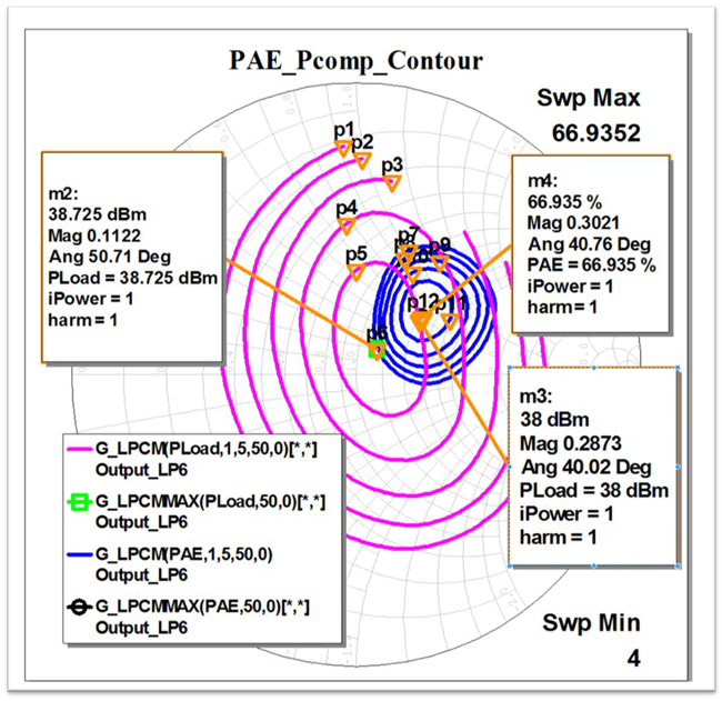
Figure 5 Load-pull contours at 1.5 GHz.
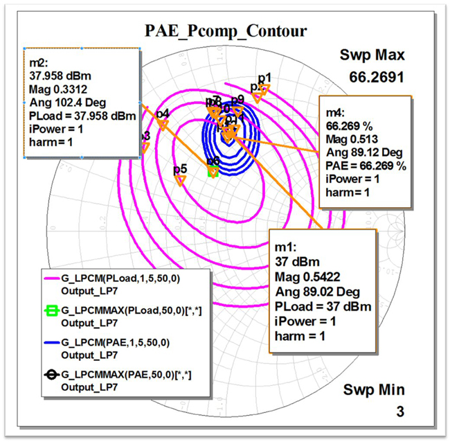
Figure 6 Load-pull contours at 5 GHz.
The BST varactor layout is shown in Figure 7. The overlapping area that produces the capacitive effect is sized at 12.5 μm x 12.5 μm, and the varactor is layered such that the bottom layer metal thickness is 750 nm, the BST layer 250 nm and the top gold 2.63 μm. A photoresist layer provides passivation to prevent oxidation. The varactors are diced from a wafer and wire bonded to the PA board.
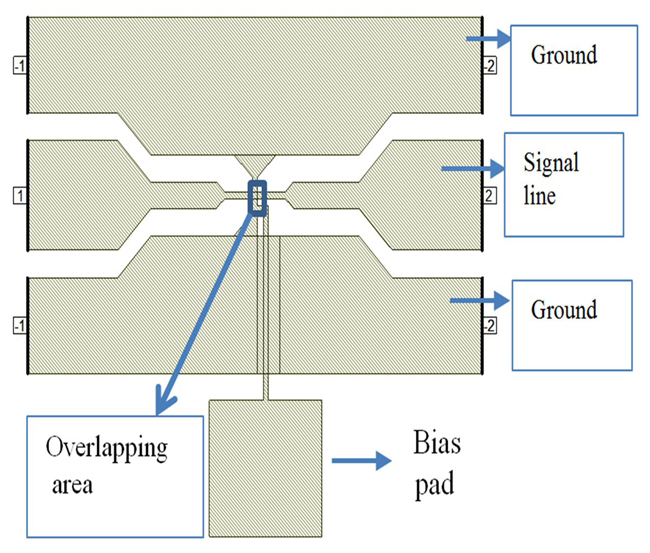
Figure 7 BST varactor layout with bias pad.