
This article describes an algorithm for the design of a voltage-controlled oscillator (VCO) with an active structure controlled by a sequential feedback circuit containing a high-quality open dielectric resonator. Its effectiveness is illustrated with the design of an X-Band oscillator that meets modern requirements for phase-locked loop (PLL) frequency control systems.

Figure 1 Oscillator topology.

Figure 2 Oscillator assembled in a housing.

Figure 3 DR equivalent circuit.
A microwave oscillator is typically based on a microwave assembly comprising an active two-port amplifier and a resonator, such as a dielectric resonator (DR). Oscillation is normally achieved with parallel feedback (FB). Design techniques for oscillators based on assemblies with parallel FB are well described by Bunin et al.1,2 Properties of active elements with inherent (i.e., internal) FB are not readily available to oscillator device developers; however, this information is not critical to the design.
In this work, we describe an oscillator development algorithm and verify its efficacy with the design of an X-Band VCO using inherent feedback. The oscillating system is formed by an open DR electromagnetically coupled to a varactor diode (VD) through a microstrip resonator (MSR). The main goal of the dielectric resonator oscillator (DRO) design is to achieve low phase noise, i.e., not to exceed -90 dBc/Hz at 10 kHz offset from the carrier. This level corresponds to or is better than the performance of similar products from leading manufacturers.3-7 The main application is low phase noise PLL frequency sources,8 where there is high interest and demand.9
OSCILLATOR DESIGN
The proposed algorithm for DRO design with inherent FB greatly simplifies DRO development. This algorithm consists of two stages: First, one creates a microstrip oscillator on a dielectric substrate using the topology and physical configurations shown in Figures 1 and 2. The required oscillation frequency is achieved by trimming the length of microstrip line (MSL) connected to the input port of the active two-port device, shown as conductor 1 in Figure 1. The oscillation frequency is measured and the length, l, of MSL 1 is recorded. Second, in the housing cup threaded hole, a screw is placed on one end of a dielectric body (e.g., a quartz cylinder) attached to a dielectric disk (i.e., a DR). Moving the case cup along the substrate axis and varying the distance between the DR edge and the substrate surface controls the electromagnetic coupling between conductor 1 and the DR. VCO implementation is enabled by adding an MSR coupled to the DR and connected to a VD.
Selection of the optimal DR position and coupling to the VD is accomplished by a simplified approach, which is demonstrated with the design of an 8 to 10 GHz DRO. The DR equivalent circuit is shown in Figure 3. The characteristics of the coupling structure are defined by the resonant frequency ƒ0 and the inherent Q-factor, Q0:
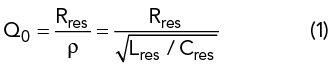
By selecting

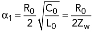
The microstrip transmission line model is described by its length, l, longitudinal resistance per unit length, R0, inductance per unit length, L0, transverse conductance per unit length, G0, and capacitance per unit length, C0. These values can be calculated knowing the MSL wave resistance, Zw; propagation constant, γ; damping in the line, α; and wavelength, λw, in accordance with following:


where λ0 is the wavelength and εeff the effective permittivity of the MSL substrate.

where
is the damping due to losses in the line metal and

is the damping due to losses in the dielectric.
For example, for an MSL on a polycor substrate with Zw = 50 Ω, √εeff ≈2.5 and known values of α1 and α2, one obtains: L0 = 0.41667 μHn/m, C0 = 0.16667 nF/m, R0 = 30 Ω/m, G0 = 0.01 Sim/m and


Figure 4 Magnitude of the MSR impedance vs. frequency, with CVD = 0.1 (a) and 0.01 (b) pF.
Figure 4 shows the calculated frequency dependence of the MSR. With a decrease of VD capacitance, by changing the VD voltage, the resonant frequency of the MSR increases, consistent with the theory.
Modeling of coupling between the DR and MSL assumes an ideal transformer (IT), which characterizes the coupling between the DR and the transmission line. The IT properties are defined by

The coupling coefficient β is determined by

Using the coupling model between the DR and MSL, one can calculate the scattering matrix coefficients, which correspond to the theoretical results obtained from the wave equations for the transmission line. The desired resonant frequency of 10 GHz is achieved by varying the VD capacitance between CVD = 0.01 and 0.1 pF respectively (see Figure 5). Changing the VD capacitance changes the electrical length of the microstrip resonator (i.e., its resonant frequency), which changes the coupling frequencies of the associated oscillator system (i.e., the entire frequency response). The entire frequency response change is quite small, on the order of several MHz.

Figure 5 Magnitude (green) and phase (red) of the MSL impedance with CVD = 0.01 (a) and 0.1 pF (b).

Figure 6 Dependence of the coupling coefficient, k, on the relative position of the DR to the MSR.
The dependence of the coupling coefficient, k, between the DR and MSR is shown in Figure 6. Lengths l3 and l4 are parts of the overall microstrip resonator length (i.e., l = l3 + l4), indicating the position of the DR with respect to the microstrip resonator.

where f1 and f2 are coupling frequencies that define the frequency tuning of the oscillator.
The frequency response curves of the oscillating system MSL-to-VD interface with various MSR lengths are shown in Figure 7. Figure 8 shows the frequency dependence of the coupling frequency, f1; the Q-factor, Q; and the transfer function versus CVD.

Figure 7 MSR frequency response vs. CV and MSR length.

Figure 8 Coupling frequency, f1, and associated Q-factor, Q1, vs. CV, with l4 = 0.2 cm (1) and 0.3 cm (2).