Application Note
Technology and Innovation in Single Layer Capacitors
Lambert Devoe and Alan Devoe
Presidio Components Inc.
San Diego, CA
Single layer capacitors have been manufactured for many years for high frequency microwave applications. The simple parallel plate structure has advantages over multi-layer capacitors up to gigahertz frequencies due to its low inductance and low effective series resistance (ESR). This article discusses the traditional method for manufacturing single layer capacitors and describes a technological innovation in the field - the buried single layer capacitor™ device.
Traditional Single Layer Capacitors
The manufacturing of traditional single layer capacitors begins with a fired ceramic substrate with a typical thickness of 0.005". The ceramic substrates use various dielectric formulations, depending on the type of capacitor that is being constructed. Next, both surfaces of the fired substrate are metallized by either a thick or thin film process. Finally the substrate is diamond sawed into square or rectangular chips. The result is a simple parallel plate, single layer capacitor structure, as shown in Figure 1 . While this type of construction has served the industry quite well for many decades, it has several disadvantages.

Fig. 1 Single layer, parallel plate capacitor.
The capacitance is limited. To understand the limits of the traditional technology, one must recall the simplified equation for capacitance
C = e0 KA/d
where
e0 = permittivity of vacuum
K = dielectric constant of the ceramic
A = overlapping surface area of the opposing electrodes
d = dielectric thickness between the electrodes
Because these single layer capacitors must maintain a certain thickness for mechanical strength purposes, the thickness d must remain large, therefore the capacitance is limited. Attempts to make the capacitors thinner than 5 mils pose several problems. For example, the manufacturing and processing of the capacitors is more difficult with thinner substrates; assembling thin capacitors poses problems associated with epoxy wicking; and the thin capacitors are susceptible to breaking under compressive force during wire or ribbon bonding.
Single layer capacitors require too many types of dielectrics. Given that the dielectric thickness d is constant in traditional capacitors, the manufacturers have had to vary the dielectric constant K in order to offer the range of capacitance needed by the end users. The result is that traditional capacitors are made from as many as 18 dielectric types, each with unique electrical properties. When the value of K is increased, there is a trade-off in which temperature, voltage or time stability, or Q factor are sacrificed.
Shorts are possible during assembly, as single layer capacitors are typically mounted using conductive epoxy. Often the result is that the epoxy oozes up the side of the device, resulting in either a short circuit or a reduced voltage rating. To correct this, the manufacturers have offered two solutions: a pulled-back metallization or a trapezoidal shaped device. These solutions offer better manufacturability, but they reduce the active area A, thereby reducing the achievable capacitance (see Figure 2 ).

Fig. 2 Possible electrical short occurence during mounting when a traditional single layer capacitor is used.
A final drawback for traditional single layer capacitors relates to capacitance tolerance. Because of small variations in the dielectric thickness d, and because the exact dielectric constant can vary in the process, manufacturers have been forced to adjust the area A in order to control the capacitance value. This is commonly done by either varying the X or Y dimension during the dicing operation. The result can be a product whose size varies from lot to lot, causing manufacturing problems with automated pick-and-place machines and pattern recognition software.

Fig. 3 Buried single layer capacitor cross-section.
New Technology
The buried single layer capacitor (BSLC) has been patented by Presidio Components Inc. (PCI) in which the two parallel and opposing metal plates are buried within the single layer device and brought to the surface by conductor-filled micro via-holes. One of the primary advantages of this technological innovation is the ability to decrease the dielectric thickness d between the two buried parallel plates. The dielectric thickness can now be 10 times thinner, or 0.0005" (see Figure 3 ). This thinner dielectric has been available in multi-layer ceramic capacitors for over a decade, but never available in single layer capacitors until now. The advantages of this new degree of freedom are:
- Greater capacitance : BSLC offers a 10 to 1 capacitance increase over equally sized, traditional single layer devices. For example: a 3030, X7R, 180 pF can now be made with a capacitance as high as 1800 pF.
- Reduced size : compared to a traditional capacitor, similar values can now be achieved in much smaller sizes. For instance, a 3030, X7R, 180 pF can be made as small as a 1010, X7R, 180 pF.
- Manufacturability : with BSLC, the end users can now receive the pulled-back border without compromising the total capacitance. In addition, capacitance tolerance variation can now be controlled with slight variation of the internal dielectric thickness, instead of varying the X and Y dimensions. The result is a part in which the X and Y size is constant, giving improved automated manufacturing.
- Use of better performing ceramic materials : the ability to change the dielectric thickness allows a greater number of capacitance values that can be made with a fewer number of better performing dielectrics. In general, this results in capacitors made with higher Q factors and better stability with temperature, voltage and time. For instance, a 3030, Y5V, 1000 pF can be made as a 3030, X7R, 1000 pF.
- High frequency performance : the final advantage, better high frequency performance, relates directly to the use of better ceramics. To understand the impact of the use of better materials in the construction of buried single layer capacitors and their relevance at high frequency, an overview of ceramic materials properties is provided.
The Electronic Industry Association (EIA) separates ceramic dielectrics into four classes, from least to most variation in capacitance versus temperature, voltage and time, as shown in Table 1 .
|
Table 1 | ||||
|
EIA Description |
Range of Dielectric Constant: K |
Approximate Q (at 1 kHz to 1 MHz) |
Maximum Drop in Capacitance (compared to 25°C) (%) |
Temperature |
|
Class I |
|
|
|
-55° C to 125°C |
|
NPO/COG |
10-20 |
12000 |
0.3 |
0 ppm ±30ppm/°C or |
|
NPO/COG Standard |
50-60 |
6000 |
0.3 |
0 ppm ±30 ppm/°C |
|
NPO/COG Standard |
80-100 |
4000 |
0.3 |
0 ppm ±30ppm/°C |
|
N80 |
70-90 |
1000 |
1.1 |
-80 ppm ±30 ppm/°C |
|
Class II |
|
|
|
-55°C to +125°C |
|
X7R |
1200-4000 |
100 |
15 |
±15% |
|
Class III |
|
|
|
various |
|
Z5U |
8000-10000 |
40 |
56 |
+22%-56% |
|
Y5V |
10000-14000 |
40 |
82 |
+22%-82% |
Class 1 materials are those whose dielectric constant is least variable with temperature, voltage and time. Components made with this type of dielectric are suited for resonant circuit applications requiring the highest quality factor (Q) and highest stability. Capacitors made with this type of material are typically low value due to the low dielectric constant (10 pF, for example), but can be made with very tight tolerances due to the overall ceramic stability (±0.1 pF, for example). This type of dielectric is designated by the familiar codes NPO, COG and negative temperature coefficient series N80 to N4700. A typical porcelain NPO dielectric has a dielectric constant K equal to 10, with a Q near 10,000 at 1 MHz. A typical N4700 has a dielectric constant K equal to 800, with a Q near 150 at 1 MHz.
Class 2 materials are those whose dielectric constants show a greater variation with temperature and voltage. Their dielectric constants are greater than that found in Class 1 materials, but their Q is lower. Capacitors made with these materials are suited for bypass, decoupling and DC blocking applications. To be included in Class 2, the material must have a temperature coefficient (TC) that is less than 22 percent from -55° to +125°C. X7R ceramic, for example, has a TC that is within 15 percent from -55° to +125°C, a Q near 100 at 1 kHz and a dielectric constant of 4000.
Class 3 materials have dielectric constants that are even greater than those found in Class 2, but with the disadvantage of even lower Q and less temperature, time and voltage stability. Capacitors made with these materials are suitable for applications where dielectric loss, insulation resistance and capacitance stability are not of major importance. The EIA defines Class 3 materials as those with temperature variation greater than ±22 percent from -55° to 125°C. These materials can typically exhibit as much as 82 percent capacitance drop at 85°C and have a Q near 40 at 1 kHz; these materials are designated by the familiar codes Z5U and Y5V.
Class 4 ceramic dielectrics are those that utilize reduced titanate ceramics combined with an insulating barrier layer. This ceramic is unlike other commonly used ceramic dielectrics in the multi-layer or single layer ceramic capacitor industry because it is based on large, semiconducting grains combined with oxide layers on the surface. This type of material is capable of giving a high dielectric constant with a stable temperature coefficient, but the performance of the material can be limited by the resistivity of the semiconducting grains of ceramic. Historically this has limited the usable frequency range of the finished capacitors (see US patent # 4761711).
Given a specific size and value, the BSLC technology often allows capacitors to be made with a dielectric class of material that the traditional technology would not permit. What follows is a summary of comparative testing of two 0.035 in.2 , 1000 pF single layer capacitors. One is made with the traditional technology using a class 3, Y5V dielectric, while the other is made with BSLC technology using the class 2, X7R material. High frequency tests were run at room temperature and at 85°C. The reader should keep in mind that, at 85°C, the capacitance of the X7R material has dropped less than 15 percent while the Y5V has dropped as much as 85 percent. The difference is shown graphically in Figure 4 .

Fig. 4 Change in capacitance vs. temperature for two classes of dielectric material.
Impact on Microwave/ mm-Wave Performance
The temperature dependence of the Y5V material will affect the microwave/mm-wave performance of a capacitor and, depending on the application, the impact may be significant. For an approximately 1.0 nF capacitor, toward the lower end of the frequency spectrum, the series resonance is at issue. At this frequency, the phase shift through the capacitor, that is, the phase of the scattering parameter, S21 , is 0° and a minimum insertion loss is generally observed. The series resonance frequency is inversely proportional to (LC)1/2 , where L is the effective series inductance of the capacitor, and thus increases as the capacitance drops. This effect is illustrated in Figure 5 for the Y5V and X7R capacitors. The resonance frequency for the Y5V capacitor increases over temperature by a factor of approximately (5.3)1/2 , which is consistent with the capacitance drop previously described (1 - 5.3-1 ≈ 80 percent). The effect of the resonance shift was to increase the insertion loss at 150 MHz from 0.03 to 0.20 dB. Comparable test data for the 1.0 nF X7R capacitor shows the constant 150 MHz resonance frequency over temperature; the insertion loss for this capacitor was approximately 0.04 dB.

Fig. 5 Phase of S21 for a 0.9 nF, Y5V capacitor and a 1.0 nF, X7R capacitor, mounted in series and measured at 25° and 85°C.
Although the resonance shift due to the capacitance variation can be readily designed around, more dramatic effects at higher frequency are much less benign. The primary use of large-valued, single layer capacitors is in broadband applications and in this arena the capacitor response must be reasonably constant, or at least changing in a monotonic fashion, over frequency. Cavity resonances, which arise when the capacitor dimensions are of the order of a wavelength, are the main source of non-monotonic behavior. In this regard, the temperature-dependent behavior of the Y5V material results in more than a simple frequency shift.

Fig. 6 Magnitude of S21 for a series-mounted 0.9 nF, Y5V capacitor and a 1.0 nF, X7R capacitor measured at 25° and 85°C.
The S21 (transmission) magnitude for the same Y5V and X7R capacitors is shown in Figure 6 , as measured in a series (DC-blocking) configuration. At 85°C, the Y5V capacitor exhibits a noticeable, periodic parallel resonance, with the first one occurring at 4.74 GHz. Using classical waveguide theory, the predicted resonant frequencies will occur at

where a, b, c are the capacitor dimensions, measured here as 30 x 35 x 4 mils3 . For c < a < b, the dominant mode frequency is f110 and by equating this to 4.74 GHz, a relative dielectric constant of approximately 2990 is obtained. This dielectric constant corresponds to a capacitance of 0.179 pF, very close to the measured low frequency value of 0.183 pF at 85°C. Subsequent resonant frequencies at 9.1 and 13.3 GHz appear to correspond to f220 and f330 , indicating that intermediate cavity effects (such as f120 ) are not as strong. Most importantly, an increase in insertion loss of up to 0.5 dB occurs at each resonance. At 25°C, however, the capacitor shows only a single, much less obvious resonance near 2.2 GHz; as expected due to the higher value for the dielectric constant, it occurs approximately (5.3)1/2 lower in frequency than the first resonance at 85°C. The X7R part exhibits no discernable change in the broadband response over temperature.
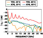
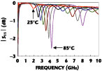
The cavity resonance behavior can be further examined by inspection of the S11 response with the capacitors mounted in a shunt (bypass) configuration. The 85°C data for the Y5V capacitor shows the resonant frequencies being nearly equal to those measured in the series configuration, but the drop in the reflection coefficient (S11) is more pronounced than the corresponding structure for S21 in the series configuration (see Figure 7 ). The cause of the apparently amplified effect is due to reduced loading on the capacitor to ground or 0 W for the shunt case versus 50 W for the series case. The parallel resonance near 2 GHz in the 25°C data is likewise more evident in this configuration. The temperature-stable X7R material exhibits nearly constant and monotonic behavior across the band, with local variation in |S11 | on the order of ±0.15 to 0.20 dB.

Fig. 7 Magnitude of S11 for a shunt-mounted 0.9 nF, Y5V capacitor and 1.0 nF, X7R capacitor measured at 25° and 85°C.
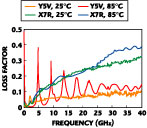
As noted, the cavity effect manifests itself as a parallel resonance. For the Y5V capacitor at 25°C, and across the temperature range for the X7R part, the resonance is a low Q response whose effect diminishes with increasing frequency; for the shunt configuration the resonance is only discernable by broad peaks in S21, which were generally at the -30 dB level and below. At 85°C the Y5V capacitor has noticeable power dissipation that leads to the drops previously illustrated, which corresponded to more narrow peaks in S21 at the -10 to -15 dB level (see Figure 8 ). Thus, the stable capacitance and quality factor of the X7R material results in monotonically varying broadband performance, at the expense of some increase in loss. For the Y5V capacitor, the cavity resonance effect increases with temperature, leading to pronounced frequency variation (Figure 9 ). The effects are summarized in Figure 10 , which shows the loss factor (1-|S11 |2 - |S21 |2 ) for the shunt capacitor measurements and the strong peaks in power dissipation for the 85°C, Y5V data.

Fig. 8 Magnitude of S21 for a shunt-mounted 0.9 nF, Y5V capacitor and a 1.0 nF, X7R capacitor measured at 25° and 85°C.

Fig. 9 Magnitude of S11 for a shunt-mounted 0.9 nF, Y5V capacitor as a function of frequency and temperature (in 10°C steps).

Fig. 10 Loss factor of Y5V and X7R capacitors measured in a shunt configuration at 25° and 85°C.
Conclusion
The buried single layer capacitor technology breaks the industry-wide, product offering homogeneity. Where previously constrained by traditional manufacturer's part sizes, capacitance values, corresponding dielectric material offerings and high frequency performance, end users now have a set of meaningful choices. Paramount in this new selection process is ceramic dielectric material; end users can now choose between standard single layer capacitors or those in better classes of materials using the BSLC technology. This fact offers new degrees of freedom to the industry and will drive additional comparative studies of performance.
Acknowledgments
The authors would like to thank Modelithics Inc. for their valuable assistance with microwave characterization and data analysis.
Lambert Devoe is a product manager with Presidio Components Inc., where he has worked for seven years. He holds a BS degree from the Massachusetts Institute of Technology. He is co-inventor of the buried single layer technology.
Alan Devoe is an engineering manager with Presidio Components Inc., where he has worked for 13 years. He holds BS and MS degrees from the Massachusetts Institute of Technology. He is co-inventor of the buried single layer technology and holds several patents (some are pending) in the field of ceramic devices.
