As WIN Semiconductors marks its twentieth anniversary, we look back at how III-V technology has evolved to meet continually changing market requirements and achieve production scale.
Over the last 20 years, products based on III-V semiconductor technology have transitioned from defense-oriented niche applications to an enabling technology used in mobile devices, wireless networks, satellite communications and optoelectronics. Common to all these uses is the need for economically viable solutions with best-in-class front-end performance, including operating frequency, power, efficiency and linearity. In all these applications, the performance advantages of compound semiconductors have enabled GaAs to become the dominant front-end technology for the mobile communications that connect billions of people across the globe.
The broad adoption of compound semiconductor technologies by the wireless industry is well illustrated by its remarkable revenue growth (see Figure 1). This figure, courtesy of Strategy Analytics, illustrates the impact of two macro trends on annual GaAs component revenues. The first growth phase, from 1990 to 1999, was driven by the Microwave and Millimeter Wave Integrated Circuit (MIMIC) and Microwave and Analog Front-End Technology (MAFET) programs funded by the U.S. Department of Defense, to mature critical GaAs technologies. These programs largely benefited U.S. GaAs manufacturers, helping component revenue increase from some $250 million in 1990 to $2.5 billion in 1999.
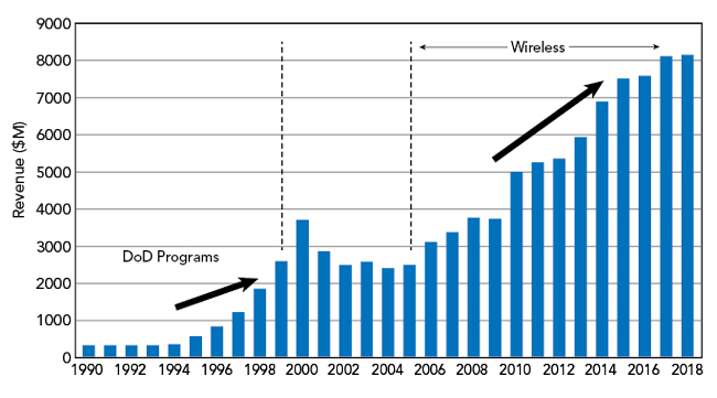
Figure 1 RF GaAs component revenue from 1990 through 2018. Source: Strategy Analytics.
The second growth phase, from 2006 to 2017, was driven by the global adoption of GaAs technology in wireless communications systems and mobile devices. Early in this period, smartphone manufacturers recognized that GaAs power amplifiers (PA) provided the optimum combination of higher linearity and transmit power with the low power consumption needed in battery-operated devices. At the same time, WIN Semiconductors provided pure-play foundry access to a portfolio of GaAs technologies. The superior performance and value of GaAs front-ends combined with rapid production scaling enabled the industry to support annual smartphone shipments exceeding 1 billion units, with RF GaAs revenue more than $8 billion in 2017.
PURE-PLAY FOUNDRY MODEL
An underappreciated element in the market uptake of III-V products was the success of the pure-play foundry model. When WIN Semiconductors started in 1999, the III-V wafer foundry business was exclusively a side business of the established GaAs component manufacturers. This made good economic sense for the foundry owner, selling excess wafer capacity to an external component company increased fab utilization, and the added revenue offset some of the fixed costs of a capital-intensive factory. This was a viable foundry model as long as there was no direct competition between the wafer supplier, an integrated device manufacturer, and the foundry customer, also an integrated device manufacturer.
Inevitably, component suppliers with similar product expertise will compete for the same market opportunities. This competition typically results in lost business for the foundry customer, because fabless component suppliers are at a significant disadvantage when they compete with their foundry suppliers. A wafer foundry business based on selling excess capacity inevitably creates business risk for the foundry customer and is not sustainable. Today, nearly all integrated device manufacturers have terminated their foundry businesses; the few that remain limit engagement to “strategic customers.”
To support the demand driven by the wireless industry, the GaAs component market needed access to high performance compound semiconductor technology from a pure-play foundry. WIN Semiconductors entered the III-V wafer foundry market to meet this need. To prove the pure-play model could succeed with compound semiconductors, WIN had to provide technologies that offered a market advantage: in PA performance, multifunctional integration and flexible large-scale manufacturing.
MOBILE DEVICES: EFFICIENCY MATTERS
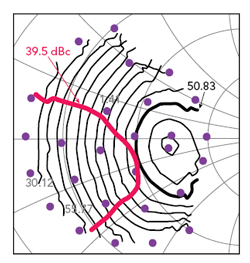
Figure 2 Impedance for peak ACLR with high PAE.
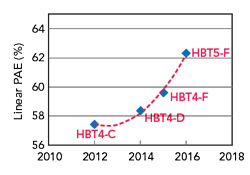
Figure 3 Linear PAE improvement for WIN HBT processes.
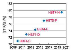
Figure 4 Improvements in HBT PAE with ET.
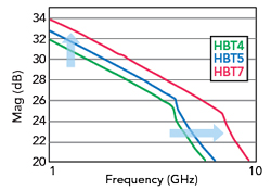
Figure 5 Small-signal gain vs. frequency for recent HBT platforms.
By the mid-2000s, broad deployment of 3G networks and mobile data services moved handsets from a business tool to a consumer device. CDMA networks imposed new linearity requirements, difficult to achieve with Si PAs. The battery limitations of mobile devices required the front-end PA to meet this linearity specification at the required power level - typically 28 dBm - while operating at the highest possible power-added efficiency (PAE). These challenging mobile PA requirements created an opportunity for high performance GaAs HBT technology. HBT quickly became the “best value” mobile PA technology, as it provided high gain (10 dB per stage), linearity (ACPR ≤40 dBc) and PAE (>65 percent), ensuring long battery life.
CDMA mobile PAs have a simultaneous set of requirements, where the primary trade-off is between linearity and efficiency at a set output power. This trade-off is shown in Figure 2, which overlays 1.95 GHz load-pull contours of PAE and linearity for an HBT2 power cell at 28 dBm output and biased at 3.4 V. HBT2 was WIN’s workhorse platform for mobile PAs from 2004 through 2008. The Smith chart shows that the loads for peak ACLR and PAE are similar, with an optimal trade-off at the intersection of the peak ACLR and the contour corresponding to 50.8 percent PAE. The output match for peak linearity is only 5 percentage points away from the peak PAE match, which is a unique characteristic of GaAs HBTs. This reduces the “cost” of efficiency to achieve linearity, enabling a compact two-stage GaAs HBT PA to meet all CDMA requirements while maintaining approximately 50 percent PAE.
With the growing popularity of high-end smartphones with large, power-hungry displays - and thin form factors limiting battery capacity - handset manufacturers expect component suppliers to reduce power consumption. To be competitive, component suppliers create differentiation by offering better performance or greater functionality with reduced current consumption. In the RF front-end, PA efficiency, linearity and functionality are the primary differentiators, and securing market share on the next smartphone platform frequently comes down to PA efficiency and the proven ability to improve performance with each design cycle.
WIN Semiconductors has responded to these expectations with successive generations of GaAs HBT transistor designs and process platforms that increase linear PA efficiency. Since 2012, WIN Semiconductors has used letter designations for production epitaxial designs, and Figure 3 compares the C, D and F epi used on the HBT4 platform. Epi C rolled out in 2012 for LTE, epi D in 2014 for improved linearity and epi F in 2015 for the higher voltage operation required for envelope tracking (ET). Comparing data from identical cell layouts and testing, all improved linear PAE, with the maximum PAE at -40 dBc ACPR. Further RF performance improvement can be achieved by shrinking device geometries. Figure 3 also shows an additional 2.5 points of PAE obtained using the HBT5 platform with epi F.
WIN Semiconductors’ HBT technologies have sustained increased linear PAE, supporting the transition from 3G to 4G and meeting increasingly difficult front-end specifications. Until 2013, average power tracking was the de-facto standard for cellular PA designs. ET was introduced to further reduce PA power consumption, and Figure 4 shows the 10-year increase in PAE for WIN Semiconductors’ HBT technologies characterized for ET. HBT7-H is WIN Semiconductors’ most advanced HBT platform, planned for release mid-year 2020.
WIN Semiconductors continues to improve HBT technology to meet the emerging demands for 5G handset PAs, which will operate to 6 GHz. Figure 5 shows the improvement in unit cell small-signal gain for several generations of HBT platforms, using the same epi. The HBT7 release will be accompanied by new epi layer designs to improve performance in the higher frequency 5G bands.
MULTI-MARKETS: POWER & EFFICIENCY MATTER
Multi-market applications for III-V technologies encompass a diverse set of functions - PAs, low noise amplifiers, RF switching, single-chip front-ends, mixers - and performance specifications - power, linearity, efficiency, noise figure and switching speed. Operating frequencies range from 1 to >100 GHz, and the diversity of products using GaAs and GaN technologies is staggering: macrocell and small cell base stations; mmWave phased arrays for 5G fixed wireless access and mobile; backhaul links; terminals for low earth orbit (LEO) and geostationary earth orbit (GEO) satellites; S-, C- and X-band radar; mmWave components in optical networks. New functions, specifications and frequencies are constantly evolving with these markets.
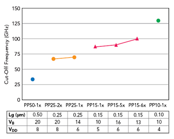
Figure 6 GaAs PHEMT cut-off frequency.
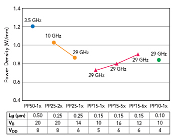
Figure 7 GaAs PHEMT transistor power density.
No single transistor technology or process node has the capability to provide the best product performance across this diverse range of functions and operating frequencies. A range of GaAs PHEMT and RF GaN HEMT technologies have proven the best options for designers. The primary figure of merit for these technologies is the cut-off frequency (ƒt), an indication of transistor capability. ƒt reflects multiple device geometry and process parameters, the most pertinent being operating frequency, output power, operating voltage and gate length (lg). Figures 6 and 7 show transistor ƒt and saturated output power in several of WIN’s GaAs PHEMT processes optimized for multi-market applications. The tables with each figure show the main transistor characteristics for each process, with the processes arranged by decreasing lg and, for the same lg, earliest to latest process. Each process was optimized for a specific multi-market requirement: PP50-1x for 10 to 20 W PAs operating below 5 GHz; PP25-2x for 10 W MMICs operating through 10 GHz; PP25-2x with higher ƒt for 30 GHz applications. With an ƒt above 90 GHz, the PP15 family supports PA MMICs through 60 GHz, and the 0.1 μm PP10 process is used for applications through 100 GHz.
Figure 6 illustrates the trend between smaller gate length and increasing ƒt. This is not the only path, as seen with the three PP15 processes. Originally released in 2001, PP15-1x operates at 5 V VDD and provides a saturated output power (Psat) of 0.7 W/mm (see Figure 7). Responding to the need for higher output power, the PP15-5x process was released in 2011, achieving a Psat of 0.8 W/mm at 6 V bias and a modest improvement in ƒt. Most recently, linearity has become a differentiator, which drove the development of PP15-6x. Released in 2018, this technology maintains 6 V operation, increases ƒt to 100 GHz, raises Psat to 0.9 W/mm and significantly improves linearity.
