
TECHNICAL FEATURE
Finite Element Determination of the Intrinsic Small-signal Equivalent Circuit of MESFETs
The finite element time domain method is used to determine the intrinsic elements of a broadband, small-signal equivalent circuit (SSEC) of FETs. The values of the different elements are calculated from the Y parameters of the intrinsic MESFET, which are obtained from the Fourier analysis of the device transient response to voltage-step perturbations at the drain and gate electrodes. The success of this analysis depends on the accuracy of the values calculated for the instantaneous currents at the electrodes during the transient. This method was applied to determine the SSEC of a 0.5 µ m gate-length GaAs MESFET.
M. Kameche and M. Feham
University of Tlemcen,
Department of Electronics
Tlemcen, Algeria
Usually, the SSEC of a FET is designed by choosing a topology, so that each element provides a lumped approximation to some physical aspect of the device. A commonly accepted SSEC is formed of fifteen different frequency-independent elements, eight of which correspond to the external parasitic effects and are normally considered independent of the bias point. The other seven describe the intrinsic behavior of the FET and are dependent on the biasing conditions. In this article a theoretical procedure is described to calculate the intrinsic elements of the FET SSEC, starting from the Y parameters obtained by using a finite element method (FEM) simulation. The FEM includes all the mechanisms relevant to the charge transport in small semiconductor devices (non-stationary effects and velocity overshoot).
For a given operating point, the Y parameters are obtained from the Fourier analysis of the device transient response to voltage-step perturbations at the drain and gate electrodes. The validity of the intrinsic SSEC proposed can be verified by checking the frequency dependence of the calculated elements.
THEORETICAL ANALYSIS
In this technique, the Fourier decomposition of the FET response to transient excitations is employed. Supposing that over the stationary operating point, a voltage-step perturbation of amplitude ΔVj is applied at electrode j, and that Ii (t) is the current response at electrode i. The complex Yij parameter will be given by the relation between the Fourier components of both signals, and can be shown to be1


where
Ii (0) = stationary current at electrode i before the voltage perturbation
Ii () = stationary current at electrode i after the voltage perturbation
Figure 1 shows the small-signal equivalent circuit of the intrinsic FET, where Cds , Cgs and Cgd correspond to the drain-source, gate-source and gate-drain capacitances, respectively. Ri is the resistance of the ohmic channel between the source and the gate. gds is the drain conductance.
|
|

For a given bias point, the elements of this intrinsic equivalent circuit can be obtained from the complex Y parameter corresponding to that point.
gm = gm0 exp(jω )
)
where
|
gm0 |
= |
steady-state transconductance |
|
|
= |
delay time of the transistor |
|
gds |
= |
drain conductance |
The Yij parameters are given by a simple circuit analysis:2 In the following, i=1 stands for the gate and i=2 for the drain.

Y12 (ω) = jωCgd (4)

Y22 (ω) = gds + jω(Cgd + Cds ) (6)
with
D = 1 + ω2 C2 gs Ri 2
From these expressions, and separating Y parameters into their real and imaginary parts, the equivalent circuit elements can be found analytically as


gds = Re [Y22 ] (13)
PHYSICAL MODEL
Short-gate-length MESFETs have been modeled using a two-dimensional geometry. The model allows a flexible description of the device with the appropriate doping and mobility. The classical semiconductor equations assume that the carrier velocities are an instantaneous function of the local electric field and that the mobility and diffusion coefficients are functions of the electric field alone (some models take into account further temperature dependence). Here, the mobility and diffusion coefficients depend on lattice temperature and carrier concentration. The model requires the solution of two nonlinear partial differential equations Poisson's equation and the continuity equation.

where
|
V |
= |
electrostatic potential |
|
q |
= |
electric charge |
|
ε0 εr |
= |
dielectric permittivity |
|
N |
= |
electron concentration |
|
ND |
= |
donor doping density |

where  , the electron current density, is given by

where
|
|
= |
electron velocity |
|
Dn |
= |
electron diffusivity |

 is the electric field, obtained directly from the potential using the relationship

The current I following at the terminals of the device is usually found by integrating the total current density J over a suitable surface enclosing each contact.

where
 = total current density obtained by adding the displacement current to the carrier current density

|
|

The present model simulates hot electron transport properties by using nonlinear steady-state velocity and diffusivity curves in the current continuity equation. The velocity-field curve of intrinsic GaAs (ND = 0)(Figure 2) is analytically approximated for the DC and AC model as3

where
|
|
= |
saturation velocity |
|
µ0 |
= |
low field mobility |
|
EC |
= |
critical field |
Or as in Roderick et al4
 (E) = µ0 E + (AE4 + Vsat )/
(µ0 E + AE4 + Vsat ) (21)
with
A µ0
µ0  5 1025 V/cms2
where A is a constant
The choice of a suitable diffusivity model poses some fundamental problems. As is well known, for fields below the threshold field, the diffusivity can be defined through a generalized Einstein relationship

where
Kb = Boltzmann constant
Tn = electron temperature assumed isotropic
This relationship becomes invalid for E>EC . In this case, the diffusivity may be modeled as an Einstein relation in lattice temperature T with one additional Gaussian term to give4

The diffusivity dependence on the electric field has been computed according to Equations 22 and 23. Figure 3 represents a comparison between these results and those obtained from the Monte Carlo simulations of Pozela and Reklaitis.5
|
|

FET PROGRAM
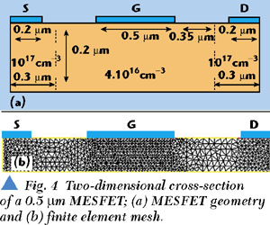
This program contains the implementation of Poisson's equation and the current continuity equation in discrete form by the use of the FEM.6 A self-consistent solution to the two equations is found by using a Scharfetter-Gummel approach,7 where Poisson's equation and the current continuity equation are solved after each time step until the solution has converged. This approach has the advantage of reducing the required core memory in the computer, in comparison to the coupled approach using a Newton-Raphson algorithm, where the two equations are treated together as a single equation. The iterative procedure is repeated until self-consistent values of desired accuracy are obtained for all unknown variables. Dirichlet (fixed value) and Neumann (zero normal derivative) boundary conditions for the potential are applied, respectively, at the contacts and elsewhere on the device surface. The initial conditions for the simulation are either derived from the electron and potential distributions in previous runs, or, for the internal nodes, the potential is set to zero with the electron distribution set equal to the doping density. A variable mesh spacing is used to optimize speed and accuracy of the solution, as shown in Figure 4. The mesh spacing criteria was based on the potential difference between the mesh nodes. The space steps are restrained to a maximum of a Debye length in the active channel, and for numerical stability it has been found that an average step width of around 0.02 µm in the active channel is necessary for a doping level of 1 x 1017 cm3 .
|
|
In order to achieve a physically meaningful solution, the time step Δt is limited to less than the dielectric relaxation time, and to avoid degrading the accuracy of the numerical solution, Δt is usually selected to lie in the range of 10 to 25 fs.
RESULTS AND DISCUSSION
Steady-state Results
Figure 5 shows the comparison between the computed current-voltage characteristics for both the FEM and the Monte Carlo (MC) simulations.1
|
|

The gate voltage includes the built-in potential of the Schottky contact (0.7 V). After a short linear dependence, a saturation region appears due to the transfer of carriers to the upper valleys. Figures 6 and 7 show the detailed potential and electron distributions for the MESFETs at two gate points VGS = 0.25 V and 1 V, respectively, with a drain voltage of 1.5 V. While the potential distributions indicate little change in form for the two bias conditions, the distributions are altered significantly by the gate potential. At large bias values a "domain" forms under the gates of the FETs in agreement with the results obtained in previous calculations. This phenomenon of the electron distribution is illustrated in the figures. A significant electron accumulation was found, which is caused by the larger region of negative differential resistance. The accumulation region gradually disappears with increasing gate bias until the domain is completely diminished and the channel is depleted and pinched-off.
 |
 |
Transient Data
The device was also analyzed with regard to its transient behaviors. In order to determine the four Y parameters, two excitations are required one in the gate voltage and the other in the drain voltage. It must be stressed that the voltage-step amplitude must be sufficiently small so as to avoid harmonic excitation in the device response, but large enough to get significant variations in the currents that dominate over numerical and physical noise. ΔV1 = 0.125 V for the case of the gate and ΔV2 = 0.5 V for the case of the drain. Figure 8 illustrates the transient response of the gate and drain currents at the bias point VGS = 1.2 V, VDS = 1.5 V.
|
|

A significant source current was found only during the first 1 ps after the step was applied. This spike is proportional to the time derivative of the applied voltage perturbation and is pure displacement current. The correct evaluation of these current spikes is essential.1 In the present case, this is assured by the value adopted for the time step (20 fs) in the simulation, which is small enough for this purpose. The duration of the transient changes depending on the operating point. The intrinsic Y parameters were obtained from the transients by means of Equations 1 and 2.
The final step in this procedure is to apply Equations 7 to 13 to the previous Y parameters in order to determine the values of the SSEC elements. The dependence on frequency of the intrinsic elements obtained in this way is shown in Figure 9. Before averaging the parameters over frequency, the relative parameter, defined as an offset plus the parameter at frequency point divided by the average, is plotted versus frequency. It can be observed that all of them are in constant frequency at least up to 60 GHz. This means that the proposed SSEC describes correctly the AC behavior of the MESFET for this bias point, where the drain current is not very high and the accumulation of carriers between the gate and the drain is not important.
|
|

The value of cut-off frequency fT can be calculated by dividing gm by (Cgs + Cgd ), which gives fT = 43.7 GHz. The cut-off frequency computed by the Monte Carlo simulations1 is about 44 GHz.
CONCLUSION
A finite element method for the calculation of the FET SSEC has been described and applied to MESFETs. The method consists in the excitation of the different elements from the frequency dependent Y parameters of the intrinsic FET, obtained from the Fourier analysis of the device transient reponse to voltage perturbations at the terminals. Finally, the FEM, which uses a correcting factor to model the field-dependent diffusivity-to-mobility ratio, has been a powerful tool to check the validity of small-signal models. *
References
1. Tomas Gonzalez and Daniel Pardo, "Monte Carlo Determination of the Intrinsic Small-signal Equivalent Circuit of MESFETs," IEEE Transactions on Electron Devices, Vol. 42, No. 4, April 1995.
2. G. Dambrine, A. Cappy, F. Heliodore and E. Playez, "A New Method for Determining the FET Small-signal Equivalent Circuit," IEEE Transactions on Microwave Theory and Techniques, Vol. 36, July 1988, pp. 11511159.
3. J.G. Ruch and G.S. Kino, "Transport Properties of GaAs," Physics, Vol. 174, pp. 921931.
4. Roderick W. Mccoll, Ronald L. Carter, John Mowens and Tsay-Jiu Shieh, "GaAs MESFET Simulation Using PISCES with Field Dependent Mobility-diffusivity Relation," IEEE Transactions on Electron Devices, Vol. 34, No. 10, October 1987.
5. J. Pozela and A. Reklaitis, "Electron Transport Properties In GaAs at High Electron Field," Solid State Electronics, Vol. 23, 1980, pp. 927933.
6. M. Kameche, "Analysis and Modeling of the Microwave MESFET by Finite Element Method," Master Thesis, University of Tlemcen, Algeria, 2000.
7. L. Scharfetter and H.K. Gummel, "Large-signal Modeling of GaAs MESFET Operation," IEEE Transactions on Electron Devices, Vol. Ed-30, 1983, pp. 18171824.
|
M. Kameche received his master's degree in signal and electronic systems (communication) from the University of Tlemcen (Algeria) in 2000. His research interests include temperature effects on GaAs MESFET devices and package modeling for microwave circuit applications. M. Feham received his doctor-engineer degree in optical and microwave communications from the University of Limoges (France) in 1987, and his doctor esscience degree from the University of Tlemcen (Algeria) in 1996. Since 1987 he has been a professor of microwave and communication engineering. His research interest is in computational electromagnetic, especially in the computer modeling of microwave components. He can be reached at m_feham@mail.univ-tlemcen.dz or feham@yahoo.fr. |