An enhancement/depletion mode InGaP/AlGaAs power pseudomorphic high electron mobility transistor (PHEMT) is demonstrated for various single- and dual-supply high efficiency power amplifiers. This technology utilizes the excellent etch selectivity and surface charge screening properties of InGaP material. At 900 MHz a depletion mode (D-mode) PHEMT features output power density of 630 mW/mm with power-added efficiency (PAE) of 85 percent at 7 V, while an enhancement mode (E-mode) PHEMT features a PAE of 70 percent and higher from 2 to 7 V and high output power densities, especially at lower voltages. A D-mode InGaP/AlGaAs-based global system for mobile communications (GSM) power amplifier delivered 35 dBm of output power with associated 65.5 percent PAE and 28 dB gain at 900 MHz with a 3.2 V supply.
InGaP material is becoming increasingly popular for both PHEMT and heterojunction bipolar transistors (HBT) used in power amplifiers and various other wireless applications.14 Its advantages compared to conventional GaAs or AlGaAs include excellent etch selectivity with respect to GaAs; lower surface potential (0.2 eV, compared to 0.8 eV for AlGaAs); absence of deep levels, such as DX centers; lower surface oxidation rate due to the absence of Al; higher valence band discontinuity at the InGaP/AlGaAs hetero-interface, leading to lower leakage currents; and critical breakdown field greater than that in GaAs resulting in higher breakdown voltages. As a result, InGaP HBTs offer improved reliability and manufacturability compared to AlGaAs HBTs, and InGaP PHEMTs have a better breakdown power/PAE tradeoff than their AlGaAs counterpart.
In this article an enhancement/depletion mode InGaP/AlGaAs PHEMT is demonstrated for various types of power amplifiers operating from 2 to 7 V, such as wireless handset, car battery powered or basestation amplifiers.
DEVICE TECHNOLOGY
The E/D-mode InGaP/AlGaAs PHEMT schematic is shown in Figure 1. The process uses a double *-Si doped epitaxial structure with the In0.5 Ga0.5 P ledge, grown by metal-organic chemical vapor deposition (MOCVD). A hall mobility of 5500 cm2 /V-s at room temperature is typically achieved for this structure. The D-mode PHEMT is a single-recess device with the TiPdAu gate placed on InGaP, while E-mode PHEMT is a double-recessed device with the InGaP ledge and TiPdAu gate placed on AlGaAs. Both recesses are done by selective wet chemistry. The devices have 0.8 µm long gates, NiAuGe ohmic contacts and are passivated with plasma-enhanced chemical vapor deposition (PECVD) silicon nitride. This process requires only minor changes compared to a conventional AlGaAs PHEMT process.
|
|
|
I-V CHARACTERISTICS
Figure 2 shows the transfer I-V characteristics of 2 mm gate width E-PHEMT and D-PHEMT devices measured in the pulsed mode. The E-PHEMT has Idss = 1 mA/mm, Imax = 250 mA/mm, Vp = +0.1 V and peak Gm = 300 mS/mm, compared to Idss = 130 mA/mm, Imax = 410 mA/mm, Vp = 0.5 V and peak Gm = 310 mS/mm for the D-PHEMT, as summarized in Table 1. Figures 3 and 4 show the pulsed output I-V characteristics of these devices. Both device types feature low on-resistance, knee voltage and output conductance.
|
|
|

Breakdown voltages measured at Ig = 0.1 mA/mm are 22 and 18 V for E- and D-PHEMT, respectively. These high breakdown levels allow high efficiency operation at voltages as high as 7 V with low gate leakage levels. This ensures adequate safety margins with respect to high SWR mismatch stability and hot-electron-induced degradation.
RF CHARACTERISTICS
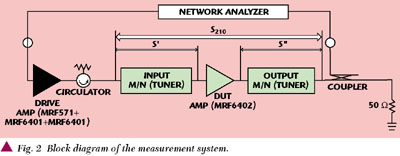
The 2 mm E- and D-mode InGaP/AlGaAs PHEMT devices are characterized at 900 MHz using an automated on-wafer loadpull measurement system, which allows independent tuning of the fundamental and harmonic impedances presented to the device output. The input and output matching are optimized for best efficiency-output power tradeoff.
The new inverted class F mode of operation5 is employed for high efficiency operation of E-PHEMT in order to compensate for its low Imax compared to the D-PHEMT. This recently proposed class of operation features an open circuit termination for the second harmonic and a near short circuit termination for the third harmonic. This results in clamping of the Id current waveform and overshooting of the Vds voltage waveform. Since the E-PHEMT technology features a relatively low Imax and high breakdown voltage, this arrangement most efficiently utilizes the available space in the output I-V plane.
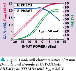
Figure 5 shows the performance of the 2 mm E- and D-PHEMT devices at Vds = 3.2 V and 900 MHz. The E-PHEMT delivers 24.5 dBm or 141 mW/mm of output power with associated PAE = 70 percent and small-signal gain of 21.4 dB, compared to 24.8 dBm (151 mW/mm) with associated PAE = 73.5 percent and small-signal gain of 22.6 dB for the D-PHEMT. The output power densities obtained are not drastically different under these high efficiency operating conditions. This is because the inverse class F operation results in the clamped Id waveform, which means the full available current swing of the device is not utilized.
|
|
|
Device performance at 7 V and 900 MHz is shown in Figure 6. The 2 mm E-PHEMT delivers 28.3 dBm or 340 mW/mm of output power with associated PAE = 82 percent, compared to 31 dBm (630 mW/mm) with associated PAE = 85 percent for the D-PHEMT.
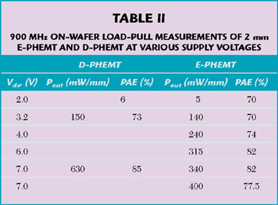
Figure 7 and Table 2 summarize the output power density and PAE for 2 mm E- and D-PHEMT at different operating voltages. A PAE of 70 percent or higher is achieved for the E-PHEMT for the whole range of voltages from 7 to 2 V. While the power density of the E-PHEMT at lower voltages is not much lower than that of the D-PHEMT, it deviates significantly at higher voltages. This occurs primarily because of the Imax limitation of the E-PHEMT, whereas the D-PHEMT can utilize the full current swing resulting in a high output power density of 630 mW/mm. At the same time, under the Vds = 7 V large-signal operation, the D-PHEMT draws the maximum average reverse gate current of 400 µA/mm, compared to 10 µA/mm for the E-PHEMT. This is a result of the drain-gate voltage excursions into the near-breakdown region and approximately 4 V higher Vbd for the E-PHEMT. For higher reliability applications the RF gate leakage can be further reduced by adopting a longer first recess on the drain side of the gate, thus increasing the breakdown voltage.
|
|
|

POWER AMPLIFIER CHARACTERISTICS
A two-stage MMIC GSM power amplifier was designed and produced based on the InGaP/AlGaAs D-PHEMT technology. The MMIC was assembled in a 16-lead shrunk small outline package (SSOP) with the output matching provided externally on the FR4 test board. Figure 8 shows the measured characteristics of this power amplifier at 900 MHz and 3.2 V. An output power of 35.5 dBm with an associated PAE of 65.5 percent and a gain of 28 dB was measured. When retuned for improved efficiency at 35 dBm power output, a PAE of 69 percent is achieved for this GSM power amplifier.
CONCLUSION
An enhancement/depletion mode InGaP/AlGaAs PHEMT for various wireless system power amplifier applications is demonstrated. An E-PHEMT features a PAE of 70 percent or higher at operating voltages ranging from 2 to 7 V. At 7 V and 900 MHz a state-of-the-art PAE of 85 percent and 630 mW/mm of output power were achieved for the D-PHEMT, while PAE of 82 percent and 340 mW/mm of output power were achieved for the E-PHEMT. To achieve high PAE, the new inverse class F mode of operation of power transistors was used. It featured an open circuit termination for the second harmonic and approximately a short circuit termination for the third harmonic on the output, which resulted in a clamped Id current waveform and overshooting of the Vds voltage waveform, an especially effective strategy for the low Imax E-PHEMT devices.
An InGaP/AlGaAs D-PHEMT GSM power amplifier delivered 35.5 dBm with associated PAE of 65.5 percent and 28 dB of gain at 3.2 V and 900 MHz. When retuned for maximum PAE, this amplifier produced 35 dBm of output power with PAE as high as 69 percent.
The demonstrated results show good promise for the InGaP/AlGaAs PHEMT technology for E-mode, D-mode or combined E/D-mode high efficiency power amplifier applications at operating voltages from 2 to 7 V.
ACKNOWLEDGMENT
This article is based on material first presented at the European Microwave Conference held in Paris, October 2000.
References
1. Y. Okamoto, K. Matsunaga, M. Kuzuhara, "E-mode Buried Gate InGaP/AlGaAs/
InGaAs HFETs Fabricated by Selective Wet Etching," Electronics Letters, Vol. 31, No. 25, Dec. 1995, pp. 22162218.
2. M. Chertouk, S. Burkner, K. Bachem, W. Pletschen, S. Kraus, J. Braunstein and G. Trankle, "Advantages of Al-free GaInP/
InGaAs PHEMTs for Power Applications," Electronics Letters, Vol. 34, No. 6, March 1998, pp. 590591.
3. M.Y. Kao, E. Beam III, P. Saunier and W. Frensley, "X-band InGaP PHEMTs with 70 Percent Power-added Efficiency," 1998 IEEE MTT-S Digest, pp. 16711674.
4. D. Geiger, E. Mittermeier, J. Dickmann, C. Geng, R. Winterhof, F. Scholz and E. Kohn, "InGaP/InGaAs HFET with High Current Density and High Cutoff Frequencies," IEEE Electron Dev. Lett., Vol. 16, No. 6, June 1995, pp. 259261.
5. C. Wei, Y. Tkachenko and D. Bartle, "Analysis and Experimental Waveform Study of Inverted Class F Mode of Microwave Power FETs," International Microwave Symposium Digest, Boston, 2000, pp. 525528.
|
|


 Yevgeniy (Gene) Tkachenko graduated from Kiev Polytechnic Institute (Ukraine) and received his BS, MS and PhD degrees in electrical engineering from Lehigh University. Currently, he is engineering manager at Alpha Industries with responsibilities in semiconductor device and process development for wireless communications.
  Yibing Zhao received his BSEE and MSEE degrees from Tianjin University, China, in 1984 and 1987, respectively. He received his master of philosophy degree from Columbia University in New York City in 1997. Zhao is a senior engineer with Alpha Industries Inc. His present research interests include III-V RF and microwave device designs and process developments.
  C. Wei graduated from the electrical engineering department at Tsing-Hua University, Beijing, in 1962, and received his PhD at the Chinese Academy, Beijing, in 1982. He was with the Chinese Academy of Sciences from 1966 to 1980 and 1982 to 1986 as a research professor responsible for development of microwave devices and circuits. Between 1980 and 1982 he received a fellowship from the A.V. Humboldt Foundation working at Aachen Technical University, Germany. From 1986 to 1988 he was a visiting professor at both the Herz-Heinrich Institute and Berlin Technical University, working in the area of opto-electronics. From 1989 to 1996 he was a senior scientist at Lehigh University. In 1997 he joined Alpha Industries as a principal engineer.
  Dylan Bartle graduated from the University of Reading, England, in 1981 with a BS honors in chemical physics. He also has a post graduate diploma in electronic and molecular properties of materials from Thames Polytechnic, London, England. From 1981 to 1986 he worked in the compound semiconductor division at GEC research laboratories in London, England. At GEC he was responsible for the development of ion implanted GaAs MESFET and diode devices for microwave MMICs. In 1986 he joined Alpha Industries and worked on many product and process development projects for discrete GaAs devices and MMICs. He has authored or co-authored several papers on GaAs device and process technology, and currently manages GaAs development engineering activities.