Figure 1: CAD representation of a single 1x8 patch element viewed from the top.
Part of the discussion for next generation wireless communication is the ability to rapidly steer beams from antenna arrays at higher frequencies. In this example, a proposed antenna1 is comprised of eight series-fed patch elements, each containing eight patches that are connected in such a way to produce both standing wave and traveling wave behavior. The array produces a single beam which may be swept in the horizontal axis of the array by varying the phasing of the signals at the inputs of the elements.
The array is evaluated for standard performance metrics such as S-parameters and gain as well as for effective isotropic radiated power (EIRP). EIRP is effectively the input power supplied to an antenna multiplied by the gain of that antenna. It indicates the total power that an isotropic antenna would have to radiate to match the signal strength of the main beam of the evaluated antenna. Simulations in this paper are performed using XFdtd® EM Simulation Software.

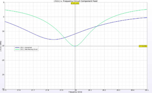
Figure 2: The Return Loss for the 1x8 element is slightly out of tune when fed with a 50-ohm source. By adding a simple LC matching circuit, the device is tuned to 28 GHz.
The final array is built from eight separate 1x8 series-fed patch elements such as that shown in Figure 1. The characteristics of a single element will be examined first before discussing the array. Each patch is 3.539 mm x 3.539 mm and is separated 3.539 mm. The last patch in the line has a notch cutout of 0.6269 mm x 2.727 mm in the connecting side. The microstrip lines connecting the patches are 0.494 mm in width. The initial feed line is 2.215 mm long and 0.72 mm wide. The total length of the element is 55.3 mm. The antenna is on a substrate with a dielectric constant of 2.2, a loss tangent of 0.0009 and a thickness of 0.254 mm.

Figure 3: The far-field gain pattern of the1x8 element has a strong central beam that is focused in one dimension and circular in other. The peak gain is just under 17 dBi.
The geometry is gridded into an FDTD mesh using the PrOGrid feature in XFdtd. Each element of the geometry has Automatic Fixed Points enabled to perfectly align the corners of the structures with the FDTD grid.

Figure 4: In the XZ dimension (E-plane) the antenna pattern has main beam with gain of 16.77 dBi and a peak side lobe level of 3.73 dBi.
The minimum feature size for Good Conductors is set to be the width of the microstrip line between patches and that is defined to have at least eight FDTD cells across it. The dielectric substrate is defined to have at least five FDTD cells of thickness using the Poor Conductor minimum feature size setting. The overall number of cells per wavelength is set to 60 to ensure good results.

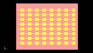
Figure 5: Shown is a CAD representation of the combination of eight of the 1x8 elements into an array. The elements are spaced 5.352 mm apart, center to center.
The input for the element is a voltage source which is initially excited by a broadband signal covering from 26 to 30 GHz for S-parameter results. Following a simulation for computing the S-parameters, the return loss is found to have a weak response due to a poor match. This is corrected by adding a matching circuit consisting of a series inductor and parallel capacitor (0.22 nH and 0.09 pF). The matched input return loss produces a null near 28 GHz (see Figure 2). The far field gain pattern for the single element (see Figure 3) indicates a strong central lobe normal to the patches with peak gain of 16.77 dBi. The peak side lobe is seen to be down about 13 dBi from the main lobe as shown in Figure 4.

Figure 6: The Return Loss of each port is shown be tuned for 28 GHz after the addition of simple LC matching circuits to each feed.
To create the array, eight of the single 1x8 elements are spaced 5.352 mm apart to form an array that measures 55.3 mm x 41 mm as shown in Figure 5. To generate broadband S-parameter data, a pulse excitation is applied to each of the eight input ports. A matching circuit similar to that used for the single element is applied to all input ports of the array. The return loss for all eight ports is seen to be very similar as shown in Figure 6, while the isolation between adjacent ports is below -15 dB for each (see Figure 7).

Figure 7: The isolation between adjacent ports is shown to be less the -15 dB for all possible combinations.
Depending on the phasing of the signals at each of the input ports, a number of different beams may be defined. When all ports are fed in phase, the beam normal to the array plane is formed with the maximum gain of 24 dBi (see Figure 8). Due to the nature of this geometry the beams may only be steered in one plane, parallel to the line of input ports. To adjust the phasing, the Butler Matrix equation is used to compute the inter-element phase difference. It is defined as:

Figure 8: The gain pattern for the array when all inputs are fed in phase results in a strong central beam with gain of 24 dBi.
αi = [(2i – 1) – M]/M * π

Figure 9: After applying Butler Matrix phase shifts to each port, a directed beam is formed. Shown are eight possible beams.
where αi is the phase difference between elements, i is the beam number or input port number of the Butler Matrix, and M is the number of ports. In this case, the phasing for beams 1-8 is -157.5 deg, -112.5 deg, -67.5 deg, -22.5 deg, 22.5 deg, 67.5 deg, 112.5 deg, and 157.5 deg. The phase shift is applied across the input ports, so the first port will have a shift of 0 deg, the second -157.5 deg, the third -315 deg, etc. for the case of beam 1.

Figure 10: The gain pattern formed from the Butler Matrix phasing for beam #1 (-157.5 degrees per port) has a broad beam with maximum gain at 55 degrees.
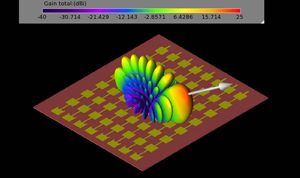
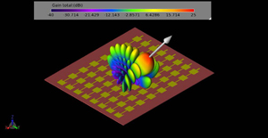
These phase shifts are applied with a sinusoidal input at 28 GHz. The resulting beams in the YZ (E-plane) are shown in Figure 9 as a series of line plots with main lobe directions of +/- 55 degrees, +/- 37 degrees, +/- 21.5 degrees, and +/- 7 degrees. In three dimensions, beams 1 through 4 may be seen in Figures 10 to 13. All eight beams are shown in one three-dimensional image in Figure 14.

Figure 11: The gain pattern formed from the Butler Matrix phasing for beam #2 (-112.5 degrees per port) has a more focused beam with maximum gain at 37 degrees. The white arrow indicates the direction of the peak gain.

Figure 12: The gain pattern formed from the Butler Matrix phasing for beam #3 (-67.5 degrees per port) has maximum gain at 21.5 degrees.
This array has been shown to form eight beams with the Butler Matrix phasing; however, a further analysis of the total gain over all possible phasing combinations is possible by computing the Cumulative Distribution Function of the Effective Isotropic Radiated Power. This plot shows the fractional area of the three-dimensional far-field sphere that the array covers for a given amount of input power.

Figure 13: The gain pattern formed from the Butler Matrix phasing for beam #4 (-22.5 degrees per port) has maximum gain at 7 degrees.

Figure 14: Shown is a side view of the eight beams produced by the Butler Matrix phasing equation. Each beam represents a separate simulation.
For this array, the CDF of EIRP plot (see Figure 15) shows that for an input power of 23 dBmW, the array has positive gain over about 27.4 percent of the far-zone sphere. This represents the scanning area where the beams have positive gain, which is limited by the ground plane under the array that blocks 50 percent of the radiation volume. The upper hemisphere of the far zone region is scanned by the beams in only one axis due to the design of the array, so therefore the scanned region is relatively limited. The plot also shows that the peak EIRP is about 46.4 dBmW.

Figure 15: The plot of the cumulative distribution function of the EIRP shows that for 23 dBmW of input power, about (1 - .726) or 27.4% of the three-dimensional far field sphere will have positive gain.

Figure 16: A Rotman Lens device suitable for use as the front end of the array is shown in Remcom’s RLD software.
As an alternative to using the Butler Matrix equations and adjusting the phases in the software, it is also possible to use a true time delay device such as a Rotman Lens in the simulation to form the beams with this array. Using Remcom’s Rotman Lens Designer® (RLD), a suitable lens (shown in Figure 16 in the RLD software) was designed to meet the criteria of the array. After exporting the CAD file of the lens from RLD and importing it into XFdtd, a complete geometry is made with eight input ports and four sidewall dummy ports (see Figure 17).

Figure 17: The resulting geometry of the array with the Rotman Lens beamforming stage are shown as a three-dimensional CAD file in XFdtd.
In the simulations the beams are created by feeding a single port at a time rather than adjusting the phasing over each port. Following eight simulations, each with a different port active, the eight beams formed by the array are visible in Figure 18. The coverage is similar to the Butler Matrix phasing shown previously in Figure 14.
Reference
- M. K. Ishfaq, T. A. Rahman, Y. Yamada and K. Sakakibara, “8x8 Phased Series Fed Patch Antenna Array at 28 GHz for 5G Mobile Base Station Antennas,” 2017 IEEE-APS Topical Conference on APWC, pp. 160-162.

Figure 18: The eight possible beam patterns from the array generated by activating one of the ports of the Rotman Lens at a time are shown.

