Figure 1 Channel of a JFET with the drain voltage equal to the pinch-off voltage (a) and the drain voltage exceeding the pinch-off voltage (b).
The efficiency of a FET is degraded when its drain voltage is greater than VDsat, the voltage at which pinch-off first occurs. Under this condition, the FET is in saturation, where the drain current is not a function of the drain voltage and is only a function of the gate voltage. To understand the degradation of efficiency, consider the behavior of a FET in saturation. When the drain voltage of a JFET, for instance, is equal to VDsat, pinch-off occurs exactly at the drain of the transistor (see Figure 1a).1 If the drain voltage is increased by ΔV, the point at which pinch-off occurs moves toward the source a distance ΔL (see Figure 1b). Over the length, ΔL, the channel is completely depleted, and the resistance is quite large. Voltage, ΔV, is dropped across this depleted region and, due to its high resistivity, ΔL is very small. For ΔL << L, which represents the usual case, depletion from the source to the pinch-off point is essentially identical in shape, and the channel has approximately the same resistance from the source to the point where pinch-off occurs. The drain current, which is equal to VDsat divided by this resistance, hardly changes. This explains why the value of the drain current is nearly constant for drain voltages greater than VDsat. Over the length, ΔL, the resistance is quite large and the power dissipated in this resistance is equal to the product of the saturated current and ΔV. The voltage, ΔV, does not contribute to output power and simply degrades efficiency.

Figure 2 Channel of a JFET with the drain voltage equal to the pinch-off voltage (a) and the drain voltage exceeding the pinch-off voltage (b).
Therefore, for high efficiency, pinch-off must be avoided, and the depletion region must be minimized. Ideally, for converting DC power to RF power, the channel should not be depleted for one-half the cycle and should be completely cut off for the other half. With an optimum load, this should yield maximum DC-to-RF efficiency. To accomplish this, a new FET has been proposed (patent pending2).
The “Grayzel” JFET
Figure 2 shows a simplified schematic of a typical JFET with a drain-to-source DC voltage of 7 V. Points along the channel have voltage values of 0, 1, 2, 3, 4, 5, 6 and 7 V, as shown in the figure. The junction is progressively back-biased by these potentials, causing greater depletion at the drain than at the source. Figure 3 shows a simplified schematic of the proposed device. The P+ region is divided into N sections that are insulated from one another, forming N, p-n junctions. As an illustrative example, in Figure 3, N = 8. Each p-n junction is biased to ground separately as shown in the figure; the first is biased at V0 and the eighth at V0 + 7 V. With a drain voltage of 7 V, all of the p-n junctions have the same DC voltage, V0, across their junctions and hence, to a good approximation, the depletion region is uniform along the channel.

Figure 3 Proposed JFET where the p-n junctions are individually biased and each junction is reverse biased at V0.

Figure 4 Simplified cross-section of the proposed MOSFET.

Figure 5 MOSFET bias network.
Dividing the gate into multiple sections is applicable to all types of FETs. Figure 4 shows an example of a MOSFET with the gate divided into N = 6 sections. Figure 5 shows a bias network with a drain voltage of 5V, biased such that each CMOS capacitor has a voltage of 5 V across it. The bias network consists of a 10 V DC voltage source and six resistors, which can be etched onto the chip.
Analysis
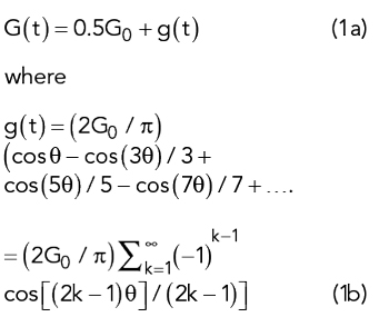
Consider a case where the odd harmonics are short circuited and the even harmonics are open circuited by the load admittance Y(ω) and where, for half of the cycle, the FET is cut off and, for the other half, the depletion region in the channel is minimum width. The conductance is thus a square wave varying between 0 and G0, where G0 is the conductance when the depletion region in the channel is the minimum width. Let θ = 2πft = ωt, where f is the fundamental frequency of the square wave. The Fourier series of the square wave is given by

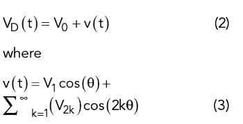
The FET is terminated in an admittance Y(ω), which at the fundamental frequency has a value GL. The value of Y(ω) = 0 at the even harmonics of the fundamental frequency and infinite at the odd harmonics. The drain voltage, therefore, has only even harmonics, and the drain current has only odd harmonics. The drain voltage, VD(t), has the form


Figure 6 FET amplifier.

Figure 7 FET amplifier equivalent circuit.
The bias voltage V0 in Equation 2 is the same for all of the segments when the proposed FET is biased as described. There is, however, a variation of the depletion region along the channel, due to v(t). This variation is small and, therefore, it is neglected in this analysis.
Equation 3 represents the voltage v(t) for the following reason. The value of the conductance of the channel is equal to G0 when −90 degrees < θ < +90 degrees, and the channel is cutoff during the remainder of the cycle; therefore, current flows only when −90 degrees < θ < +90 degrees. Since the current is equal to VD(t)G(t), VD(t) has its maximum value centered at θ = 0 degrees and is the sum of cosines.
The proposed segmented-gate amplifier shown in Figure 6 is analyzed with the aid of the circuit in Figure 7. Voltage v(t) appears across the RF choke and across the load Y(ω), which is in series with blocking capacitor C. V0 + v(t) appears across the nonlinear conductance G(t). The choke, which is in series with the DC battery, has voltage v(t) across it but negligible RF current flowing through it. Drain current ID(t) = I0 + i(t) is equal to the product G(t)VD(t). i(t) flows in a loop through the termination Y(ω). DC voltage, V0, appears across the blocking capacitor C. The drain current is given by

Equations 2, 3 and 4 yield the terms in Equation 4

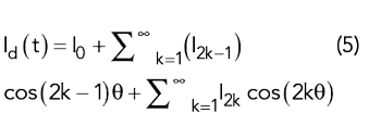
The drain current is the sum of a DC term, odd harmonics and even harmonics

Using the identity cos(x)cos(y) = 0.5[cos(x + y) + cos(x − y)] in Equation 4a, the even harmonics can be written as

Since the current at the even harmonics is zero, it is possible to solve for voltage V2k by setting current I2k = 0 in Equation 6, yielding

Collecting the terms in cos(θ) in Equation 4, the value of the current at the fundamental frequency, I1, is

Substituting Equation 7 into Equation 8 yields
![]()
The term [0.5 – (8/π2) Σ∞k=11/ (4k2 − 1)2] converges in the limit to (2/π)2 as k approaches infinity. (This limit was first estimated and then verified by a computer program.) Substituting (2/π)2 for [0.5 – (8/π2) Σ∞k=11/ (4k2− 1)2] in Equation 9 yields

At the fundamental frequency Y(ω) = GL and I1 = –(GL)(V1). Equating I1 as given by Equation 10 to –(GL)(V1), yields

where X = GL / G0 = 1 / (G0RL).
Solving Equation 11 for V1 yields

The DC current I0 is found from Equation 4 to have two terms. The first term is 0.5(G0)(V0) and the second DC term results from the product (2G0 / π)cos(V1cosθ).

Substituting Equation 12 into Equation 13 yields

The DC power is

The output power at the fundamental frequency P1 is

The efficiency, EFF, is then

Figure 8 shows a plot of efficiency as a function of X = GL / G0.

Figure 8 Amplifier efficiency vs. X.
This special case where the amplifier is terminated in an open circuit for the even harmonics and a short circuit for the odd harmonics gives good efficiency; however, it is not necessarily the optimum termination. An analysis similar to the one performed above, for the case where the amplifier is terminated in an open circuit for the odd harmonics and a short circuit for the even harmonics gives a poorer result. An optimization is warranted to determine the best termination.
SUMMARY
A FET has greater efficiency and output power if pinch-off is avoided and the depletion region is made uniform along the channel. A bias network is presented for achieving this condition for a FET whose gate is segmented. Efficiency and output power are derived for the case where odd harmonics are short circuited and even harmonics are open circuited and where for half of the cycle the FET is off, while for the other half of the cycle the depletion region is minimum width.
Acknowledgment
The author wishes to acknowledge the support provided by Ashok Gorwara, CEO, and the staff of Planar Monolithics Industries Inc.
Editor’s Note
In a future issue of Microwave Journal, we hope to publish measured data confirming this theoretical FET structure.
References
- R. F. Pierret, “Field Effect Devices: Modular Series on Solid State Devices,” Addison-Wesley Publishing Company, 1983, pp. 5–15.
- “Field Effect Transistor Which Can Be Biased to Achieve a Uniform Depletion Region,” U.S. Patent Application US20170352757A1.
